Superconducting integrated circuit and method for fabrication thereof

a technology of integrated circuits and materials, applied in the direction of superconducting magnets/coils, superconductor devices, magnetic bodies, etc., can solve the problems of insufficient reliability of insulating films, high cost of vacuum equipment, and insufficient use of low-temperature-formed silicon oxide films and silicon nitride films as the materials for conventional insulating films, etc., to reduce the number of defective parts, reduce the number of steps of process, and simplify the method of production

Inactive Publication Date: 2005-06-28
NAT INST OF ADVANCED IND SCI & TECH +1
View PDF3 Cites 5 Cited by
  • Summary
  • Abstract
  • Description
  • Claims
  • Application Information

AI Technical Summary

Benefits of technology

[0031]The superconducting integrated circuit of this invention, owing to the use of a photosensitive organic film having high-resolution characteristics of the level of microns to submicrons as an insulating film, is enabled to attain the formation of via holes in the insulating layer exclusively by the lithographic technique. Thus, the method for producing this integrated circuit is simplified through a marked decrease in the number of steps of process as compared with the conventional technique for the formation of the insulating interlayer film. By applying the high-resolution, photosensitive, organic material by the spin coating technique to the irregular surfaces of the electrodes and the wiring layers manufactured in the preceding step, thereby utilizing the excellent coating property of the material in smoothing the steps, it is made possible at the subsequent step for upper wiring to attain much reduction in the number of defective portions as by decreasing portions of steps to be climbed over. These improvements are at an advantage in enhancing the reliability of the process of wiring and exalting the yield of production of integrated circuit.

Problems solved by technology

Particularly, the changes in the characteristic properties of the junction component have a great effect as well on the operation characteristics of the superconducting integrated circuit and, therefore, have posed an important problem to be solved.
These methods invariably necessitate use of highly expensive vacuum equipment and encounter difficulty in ensuring reliability of the formation of via holes because they entail large numbers of steps.
In terms of these insulating characteristics and dielectric characteristics, the low-temperature-formed silicon oxide film and silicon nitride film that have been used as the materials for the conventional insulating films have not been fully satisfactory.
Particularly, since the silicon oxide film contains oxygen, it has proved to be an unfavorable material for the niobium superconductor that tends to induce deterioration of the superconducting property by diffusion of oxygen.
Since the formation of via holes in the insulating layer is implemented by dry etching, the wiring layer and the resistor layer which are exposed after the formation of via holes suffer loss of thickness due to dry etching and sustain damage of dry etching and consequently pose a serious hindrance to the formation of proper electrical contacts.

Method used


Image

  • Superconducting integrated circuit and method for fabrication thereof
  • Superconducting integrated circuit and method for fabrication thereof
  • Superconducting integrated circuit and method for fabrication thereof

Examples


first embodiment

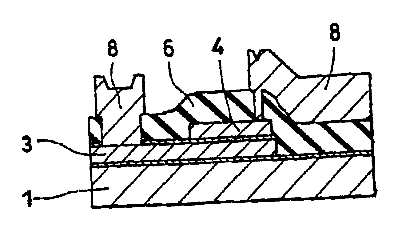
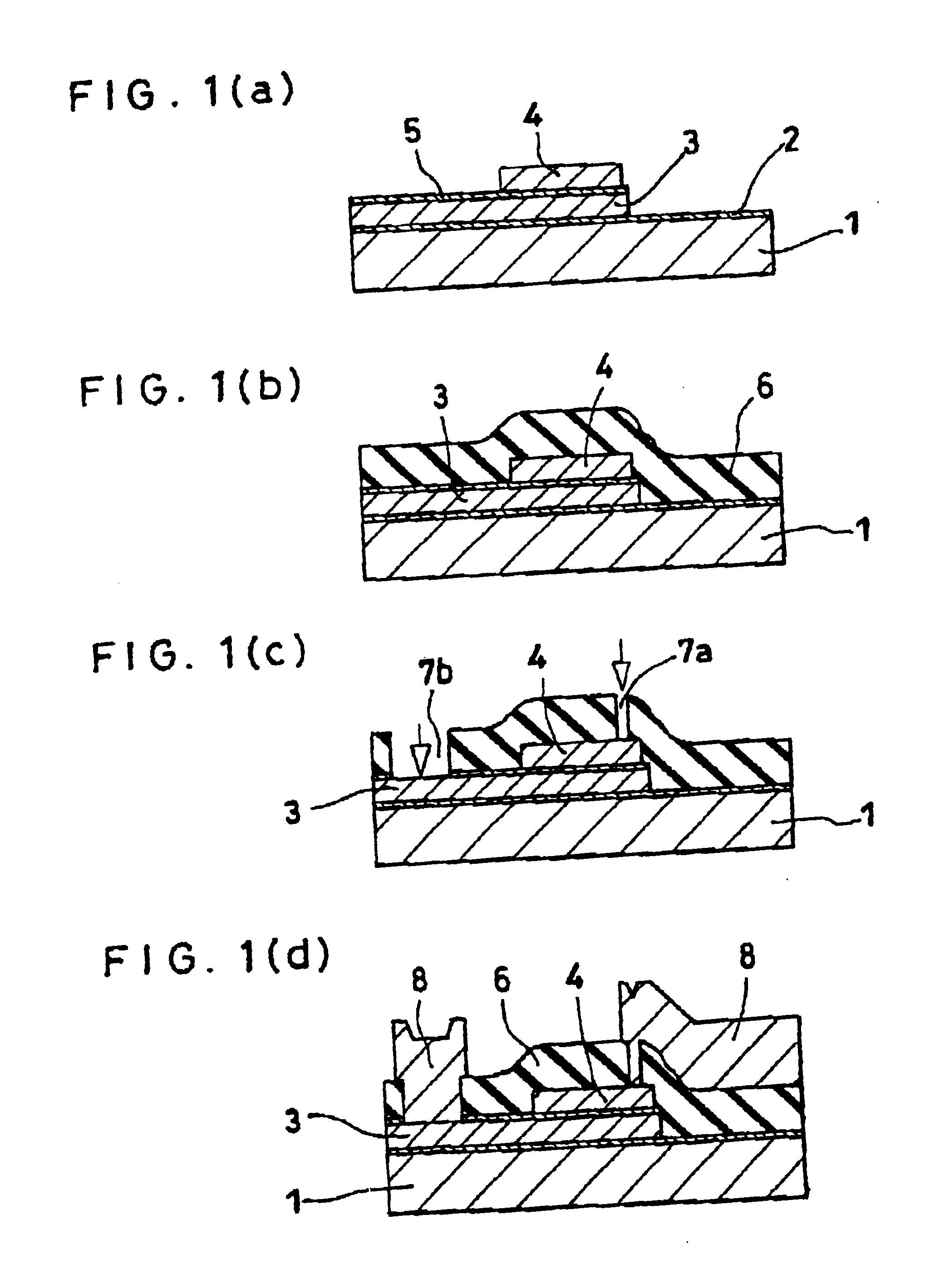
[0038]As this invention, the method for producing a superconducting tunnel device constituting a superconducting integrated circuit will be described below with reference to FIG. 1.

[0039]A protective layer 2 of MgO film against dry etching is formed on a substrate 1. A tunnel junction layer having a multilayer structure of Nb upper electrode 4 / AlOx tunnel barrier 5 / Nb lower electrode 3 is deposited thereon, then a resist pattern for the lower electrode and a twist pattern for the upper electrode are formed by the photolithographic technique. A tunnel junction layer is defined by dry etching through these resist patterns, as illustrated in FIG. 1(a).

[0040]Subsequently, a high-resolution, photosensitive, solvent-soluble, organic material, such as a photosensitive solvent-soluble block-copolyimide, is applied to the entire surface of the substrate 1 to give rise to an insulating film for insulating the upper and lower electrodes 4 and 3 from each other, as illustrated in FIG. 1(b). The...

second embodiment

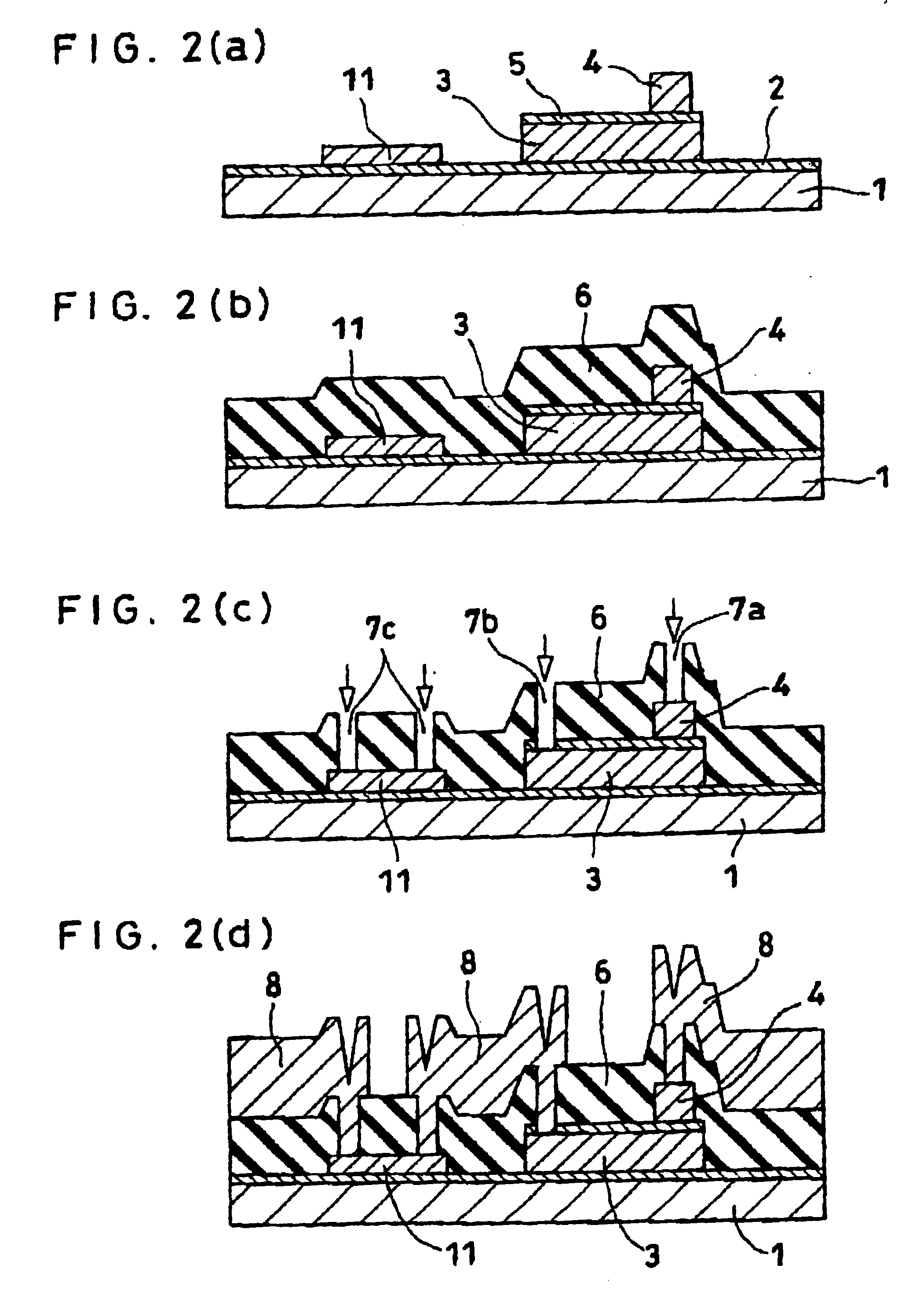
[0048]FIG. 2 depicts an example of the formation of a superconducting integrated circuit inclusive of a superconducting tunnel junction and a resistor as this invention.

[0049]First, a protective layer 2, such as of MgO, against dry etching is deposited by the evaporation or sputtering technique on a substrate 1, then a Nb lower electrode 3, an AlOx tunnel barrier 5 and a Nb upper electrode 4 are continuously formed by the sputtering technique, the lower electrode 3 and the upper electrode 4 are defined by dry etching through a resist pattern for the lower electrode and a resist pattern for the upper electrode, further a Pd resistor layer is deposited by the evaporation technique through a resist pattern for the resistor, and thereafter a fine resistor 11 is formed by the lift-off technique, as illustrated in FIG. 2(a). Incidentally, during the course of the dry etching, the etching ceases proceeding at the surfaces of the tunnel barrier 5 and the protective layer 2.

[0050]Subsequentl...

third embodiment

[0054]FIG. 3 depicts a method for producing a superconducting integrated circuit inclusive of a ground plane, a wire-bonding pad, a superconducting tunnel junction and a resistor as this invention.

[0055]First, a protective layer 2, such as of MgO, against dry etching is deposited on a substrate 1 by the evaporation or sputtering technique and then a Nb ground plane 9 is formed thereon by the sputtering technique, as illustrated in FIG. 3(a). Further thereon, a SiO2 insulating interlayer layer 10 is formed as by the sputtering technique, a protective layer 2a against dry etching is deposited by the evaporation or sputtering technique, then a Nb lower electrode 3, an AlOx tunnel barrier 5 and a Nb upper electrode 4 are continuously formed by the sputtering technique, the lower electrode 4 and the upper electrode 5 are defined by dry etching respectively through a resist pattern for the lower electrode and a resist pattern for the upper electrode, further a Pd resistor layer is deposit...


PUM


Abstract

A superconducting integrated circuit includes a substrate, a multilayer structure formed on the substrate and composed of a lower superconducting electrode, a tunnel barrier and an upper superconducting electrode sequentially joined together upward in the order mentioned, and an insulating layer perforated to form via holes to get electrical contacts with the lower and upper electrodes. The insulating layer is formed of a high-resolution, photosensitive, solvent-soluble, organic insulating material. The superconducting integrated circuit is produced by a method that includes the steps of depositing the multiplayer on the substrate, applying the insulating material to the front surface of the substrate inclusive of the multiplayer, forming the via holes in the insulating material by the lithographic technique at the prospective positions to get electrical contacts with the upper and lower electrodes, and laying wirings for connecting the upper and lower electrodes through the via holes.

Description

BACKGROUND OF THE INVENTION[0001]1. Field of the Invention[0002]This invention relates to a superconducting integrated circuit that has included superconducting components, such as superconducting tunnel junction components and microbridge components, and to a method for the fabrication thereof.[0003]2. Description of the Prior Art[0004]Heretofore, in the fabrication of a superconducting tunnel junction (Josephson) device which is an active component in a superconducting integrated circuit, a silicon oxide film or silicon nitride film has been used as the material for an insulating interlayer film intended to effect insulation between an upper electrode and a lower electrode. The insulation characteristics and dielectric characteristics of the insulating film have an effect on the signal transmission characteristics of the wiring and on the electric characteristics of the superconducting tunnel junction device as well. Particularly, the changes in the characteristic properties of th...

Claims


Application Information

Patent Timeline
Patent Type & Authority Patents(United States)
IPC IPC(8): H01L39/22H01L27/18H01L39/24H01L39/00H01L21/312H01L21/3205H01L21/768H01L23/52H01L23/522
CPCH01L27/18H01L39/2493H01L39/223H10N69/00H10N60/12H10N60/0912
Inventor AOYAGI, MASAHIRONAKAGAWA, HIROSHITOKORO, KAZUHIKOKIKUCHI, KATSUYAITATANI, HIROSHISEGAWA, SIGEMASA
Owner NAT INST OF ADVANCED IND SCI & TECH
Why Eureka
Try Eureka