Manufacture of solid state imager having plurality of photosensors per each pixel

a solid-state imager and photosensor technology, applied in the field of manufacturing methods of solid-state imagers, can solve problems such as moving objects

Inactive Publication Date: 2005-03-24
FUJIFILM CORP
View PDF4 Cites 31 Cited by
  • Summary
  • Abstract
  • Description
  • Claims
  • Application Information

AI Technical Summary

Benefits of technology

[0012] It is possible to provide a manufacture method for a solid state imager whose pixel has a plurality of photodiodes having different characteristics such as sensitivities and saturated charge amounts, the impurity profile of each type of the photodiode being able to be adjusted independently.

Problems solved by technology

However, since the exposure timings of two types of imaging are displaced, some problems occur for a moving object.

Method used


Image

  • Manufacture of solid state imager having plurality of photosensors per each pixel
  • Manufacture of solid state imager having plurality of photosensors per each pixel
  • Manufacture of solid state imager having plurality of photosensors per each pixel

Examples


Embodiment Construction

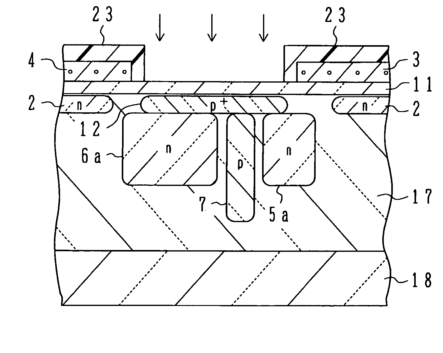
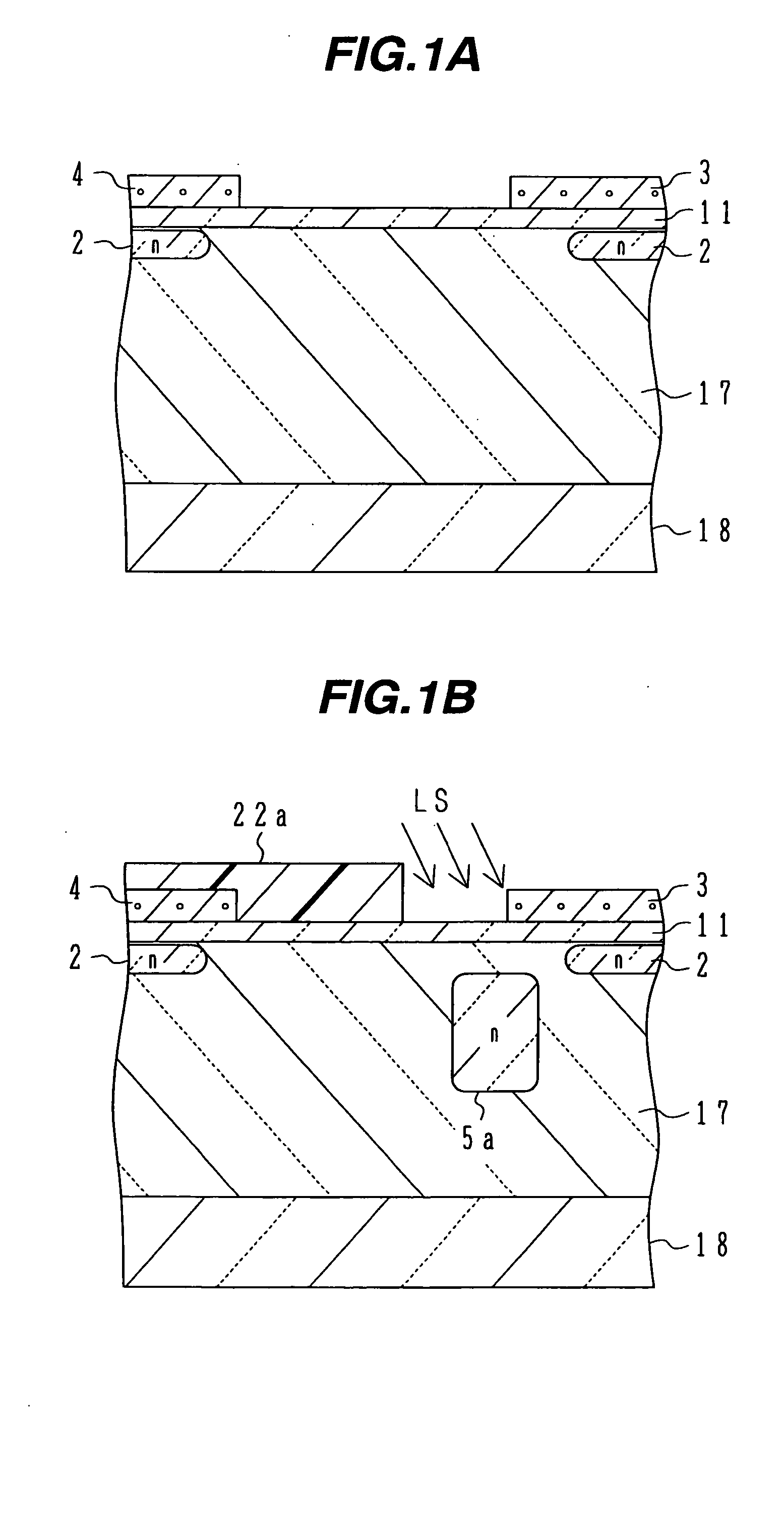
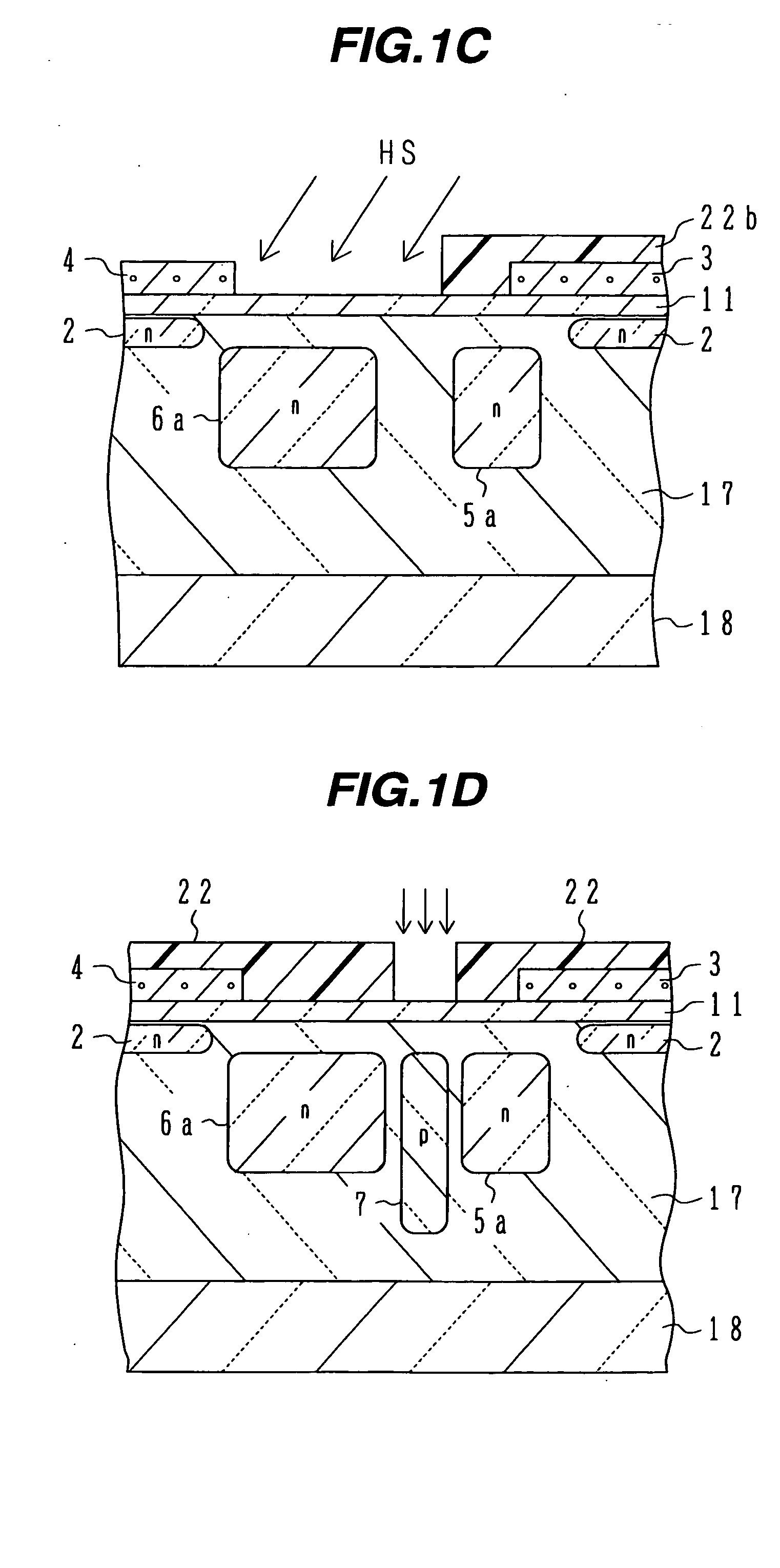
[0018] Prior to describing the embodiments of the invention, the previous proposal and its studies will be described. In a light reception area of a solid state imager, photosensitive elements, CCDs or MOS circuits, and wiring lines are disposed. These constituent elements other than the photosensitive elements are covered with a light shielding film because if light is incident upon these constituent elements, noises are generated. A micro lens is disposed above each pixel in order to make incidence light upon one pixel area be incident upon the light sensitive element as much as possible. From another viewpoint, the micro lens formed above the substrate determines each pixel area.

[0019] U.S. patent application Ser. No. ______ , assigned to the same assignee as the present application, filed on Nov. 19, 2003, and claiming priority on Japanese patent application 2002-356813, which is incorporated herein by reference, proposes a solid state imager having two or more types of photodi...


PUM


Abstract

A second conductivity type well is formed in a first conductivity type semiconductor substrate. Vertical CCD channels of the first conductivity type are formed in the second conductivity type well. Vertical transfer electrodes are formed above the vertical CCD channels to form vertical CCDs along with the vertical CCD channels. A first impurity diffusion layer is formed in the well by implanting first conductivity type impurities along a first direction crossing the normal direction of the semiconductor substrate. A second impurity diffusion layer is formed in the well by implanting first conductivity type impurities along a second direction crossing the normal direction of the semiconductor substrate. A third impurity diffusion layer of the second conductivity type is formed between the first and second impurity diffusion layer. A fourth impurity diffusion layer of the second conductivity type is formed in the well above the first to third impurity diffusion layers.

Description

CROSS REFERENCE TO RELATED APPLICATION [0001] This application is based on and claims priority of Japanese Patent Application No. 2003-327663 filed on Sep. 19, 2003, the entire contents of which are incorporated herein by reference. BACKGROUND OF THE INVENTION [0002] A) Field of the Invention [0003] The present invention relates to a manufacture method for a solid state imager whose pixel in a light reception area has a plurality of photoelectric conversion elements (photodiodes) having different characteristics. [0004] B) Description of the Related Art [0005] Various solid state imagers are known such as a charge-coupled device (CCD) solid state imager which transfers signal charges accumulated in a photosensitive element by using a CCD and a MOS type solid state imager which amplifies and outputs signal charges accumulated in a photosensitive element (converts the signal charges into voltage or current). Photodiodes are mainly used as the photosensitive elements and a number of pi...

Claims


Application Information

Patent Timeline
Patent Type & Authority Applications(United States)
IPC IPC(8): H01L27/148H01L31/10H04N5/335H04N5/369H04N5/372
CPCH01L27/14812
Inventor TAKEUCHI, YUTAKASHIBATA, KATSUHIRO
Owner FUJIFILM CORP
Why Eureka
Try Eureka