Digital compensation of excess delay in continuous time sigma delta modulators

a digital compensation and continuous time technology, applied in differential modulation, code conversion, electrical equipment, etc., can solve the problems of reducing input range, reducing the accuracy requirement of switch capacitor circuits, and reducing the clock frequency of continuous-time loop filters. achieve the effect of minimizing excess loop delay, simple and cost-effective approach

Inactive Publication Date: 2005-03-31
TEXAS INSTR INC
View PDF21 Cites 49 Cited by
  • Summary
  • Abstract
  • Description
  • Claims
  • Application Information

AI Technical Summary

Benefits of technology

Advantages of this design include but are not limited to a continuous time sigma delta converter that compensates for the excess delay in the feedback loop; wherein the analog compensation is transferred to the digital domain. This solution presents a small, simple and cost effective approach towards minimizing excess loop delay.

Problems solved by technology

Initially, most sigma-delta modulators were based on switched-capacitor circuit techniques; yet, sigma-delta modulators having continuous-time loop filters can achieve higher clock frequency and consume less power.
Higher order loops, however, cause instability problems, resulting in reduced input range.
Switch capacitor circuits, however, have drastic settling accuracy requirements requiring high bandwidth active devices consuming large current.
The first disadvantage is that continuous-time modulators are more sensitive to clock jitter.
Continuous-time modulators, however, have another substantial performance disadvantage in that continuous-time modulators include non-zero excess loop delay.
This non-zero excess loop delay presents a significant performance issue specifically when a NRZ feedback DAC is utilized within the continuous-time modulator since both the ADC and DAC have a zero input-output time delay requirement.
SNR degradation and instability may result if the excess loop delay is too large.
In particular, as shown in FIG. 2, when a constant delay τd is swept from 0 to τs / 4, the SQNR results in substantial degradation for delays higher than τs / 10.
Moreover, since the nature of a sigma delta modulator is similar to an oscillator, it is very easy to make this modulator unstable in that it will start oscillating in an undesirable way.
The delay, however, is signal dependent wherein it depends upon the signal at the output of the last integrator and, thus, will cause distortion.
If there is more than a 10% delay, there will be substantial SNR degradation.
More over this solution adds jitter and, thus, is not an effective approach.
Having signal dependent timing, however, translates into total harmonic distortion (THD) at the output of the sigma delta converter.
Specifically, if the output of the quantizer is not resampled using a clock, it will suffer signal dependent jitter.
Disadvantageously, since the time delay is dependent upon the signal, there will be THD.
Therefore, an exact solution in the s-domain is not possible.
Increasing the order of the sigma delta converter, however, will increase the complexity and power consumption without SNR improvement increase the SNR degradation.
If, however, one pole or more than one zero is added, the order will increase; and, thereby the instability of the filter will increase.
This method, however, is difficult to automate and is not reliable.
This method, however, increases the order of the transfer function.
This design is successful in minimizing the SNR and THD; however, the complexity of the design implementation incurs a substantial cost.
This approach and implementation using an analog delay may increase the distortion of the signal as well.

Method used


Image

  • Digital compensation of excess delay in continuous time sigma delta modulators
  • Digital compensation of excess delay in continuous time sigma delta modulators
  • Digital compensation of excess delay in continuous time sigma delta modulators

Examples


Embodiment Construction

The present invention will now be described more fully hereinafter with reference to the accompanying drawings, in which embodiments of the invention are shown. This invention may, however, be embodied in many different forms and should not be construed as limited to the embodiments set for the herein. Rather, these embodiments are provided so that this disclosure will be thorough and complete, and will fully convey the scope of the invention to those skilled in the art.

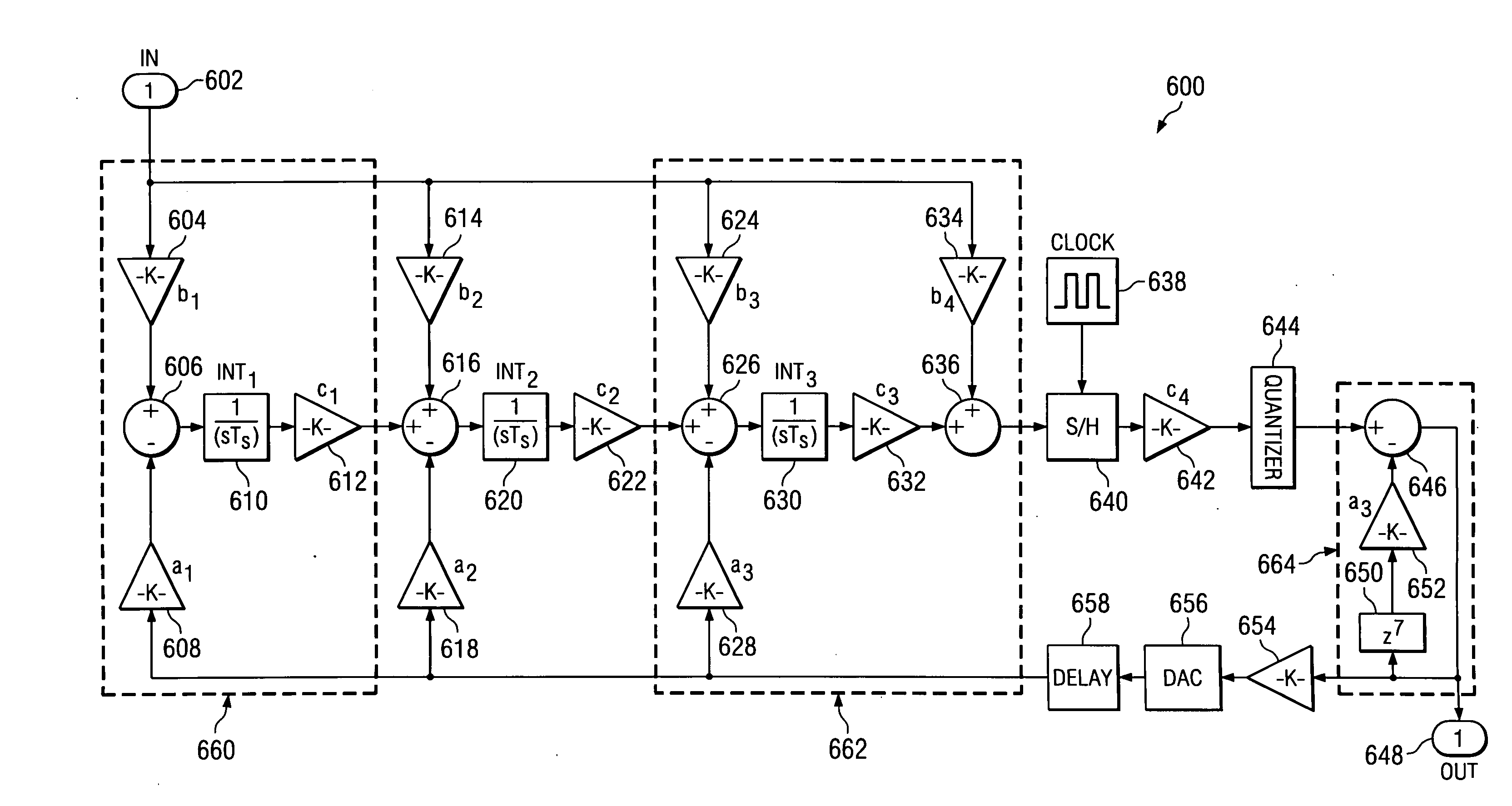
FIG. 6 illustrates the continuous time sigma delta converter in accordance with the present invention. As shown, continuous-time sigma delta modulator 600 in accordance with the present invention includes at least one integrator stage 660 coupled to receive an input signal and a resultant integrator output signal from a previous stage for providing a resultant integrator output. At least one output stage 662 connects to the at least one integrator stage 660 to receive the resultant integrator output signal from the...


PUM


Abstract

A continuous time sigma delta modulator having minimal excess loop delay. The continuous-time sigma delta modulator in accordance with the present invention includes at least one integrator stage coupled to receive an input signal and a resultant integrator output signal from a previous stage for providing a resultant integrator output. At least one output stage connects to the at least one integrator stage to receive the resultant integrator output signal from the previous integrator stage for providing a resultant integrator output. A sample and hold circuit connects to receive the second integrator input signal. A multiplier connects to the sample and hold circuit to provide a resultant sampled signal. An analog-to-digital converter quantizer couples to receive the resultant sampled signal and to produce a quantized output signal. A digital modulation loop circuit connects to the analog-to-digital converter quantizer to generate a resultant quantized output signal for correcting excess loop delay in the continuous time sigma delta modulator. A fourth feedback multiplier coupled to receive the resultant quantized output signal and produce a second resultant quantized output signal. A digital-to-analog converter coupled to receive the second resultant quantized output signal to produce a modulation feedback signal. A delay connects to the digital-to-analog converter to receive the modulation feedback signal and provide the resultant modulation feedback signal

Description

FIELD OF THE INVENTION The present invention relates to sigma delta modulators, and, more particularly, to a digital compensation of excess delay in a continuous time sigma delta converter. BACKGROUND OF THE INVENTION Conversion of analog signals to digital signals and vice versa interfaces real world systems with digital systems that read, store, interpret, manipulate and otherwise process the discrete values of sampled analog signals, many of which vary. Real world applications that convert digital signals to analog waveforms at a high resolution include systems such as, high performance audio applications, high precision medical instrumentations, codec for wireless transceiver, digital audio systems, compact disc players, digital video players, and various other high performance audio applications. Sigma-delta modulators (SDMs) have come into widespread use as a processing solution regarding these real world digital audio applications to provide a high resolution data conversi...

Claims


Application Information

Patent Timeline
Patent Type & Authority Applications(United States)
IPC IPC(8): H03M3/04
CPCH03M3/37H03M3/45H03M3/454H03M3/424
Inventor FONTAINE, PAUL-AYMERICMOHIELDIN, AHMED NADER
Owner TEXAS INSTR INC
Why Eureka
Try Eureka