Bus structure for power switching circuits

a power switching circuit and bus structure technology, applied in the field of power electronics and power switching devices, can solve the problems of circuitry operation, circuitry damage, and tendency to occur voltage spikes, and achieve the effect of reducing the parasitic conductance of circuitry and facilitating unique packaging configurations

Active Publication Date: 2005-03-31
ROCKWELL AUTOMATION TECH +1
View PDF1 Cites 210 Cited by
  • Summary
  • Abstract
  • Description
  • Claims
  • Application Information

AI Technical Summary

Benefits of technology

[0005] The present invention provides a novel bus design, and packaged circuitry incorporating such designs which respond to such needs. In accordance with aspects of the technique, a bus structure is defined by conductive planes which are placed generally parallel to one another and separate from one another and from neighboring conductors by insulative layers. The bus structure may be formed to accommodate both-single phase and multiple-phase circuitry. The technique facilitates unique packaging configurations, such as between switching devices a

Problems solved by technology

Voltage spikes tend to occur, however, during turn-on stages of operation which can be detrimental to the operation of the circuitry.
That is, as the solid state switching device is switched from a non-conducting state to a conducting state, such as to provide power to an output terminal, depending upon the configuration of the circuitry, large voltage spikes may occur which can cause damage to the switch and to other circuitry.
In many cases

Method used


Image

  • Bus structure for power switching circuits
  • Bus structure for power switching circuits
  • Bus structure for power switching circuits

Examples


Embodiment Construction

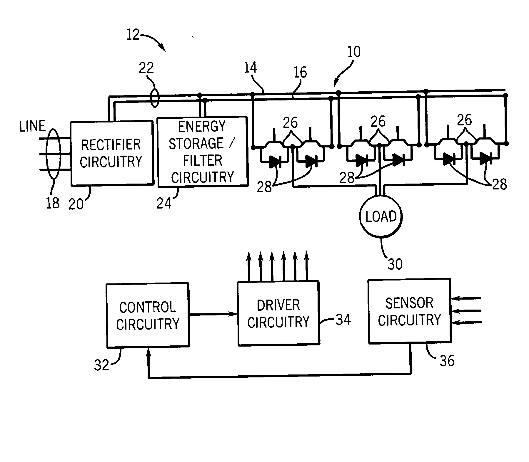
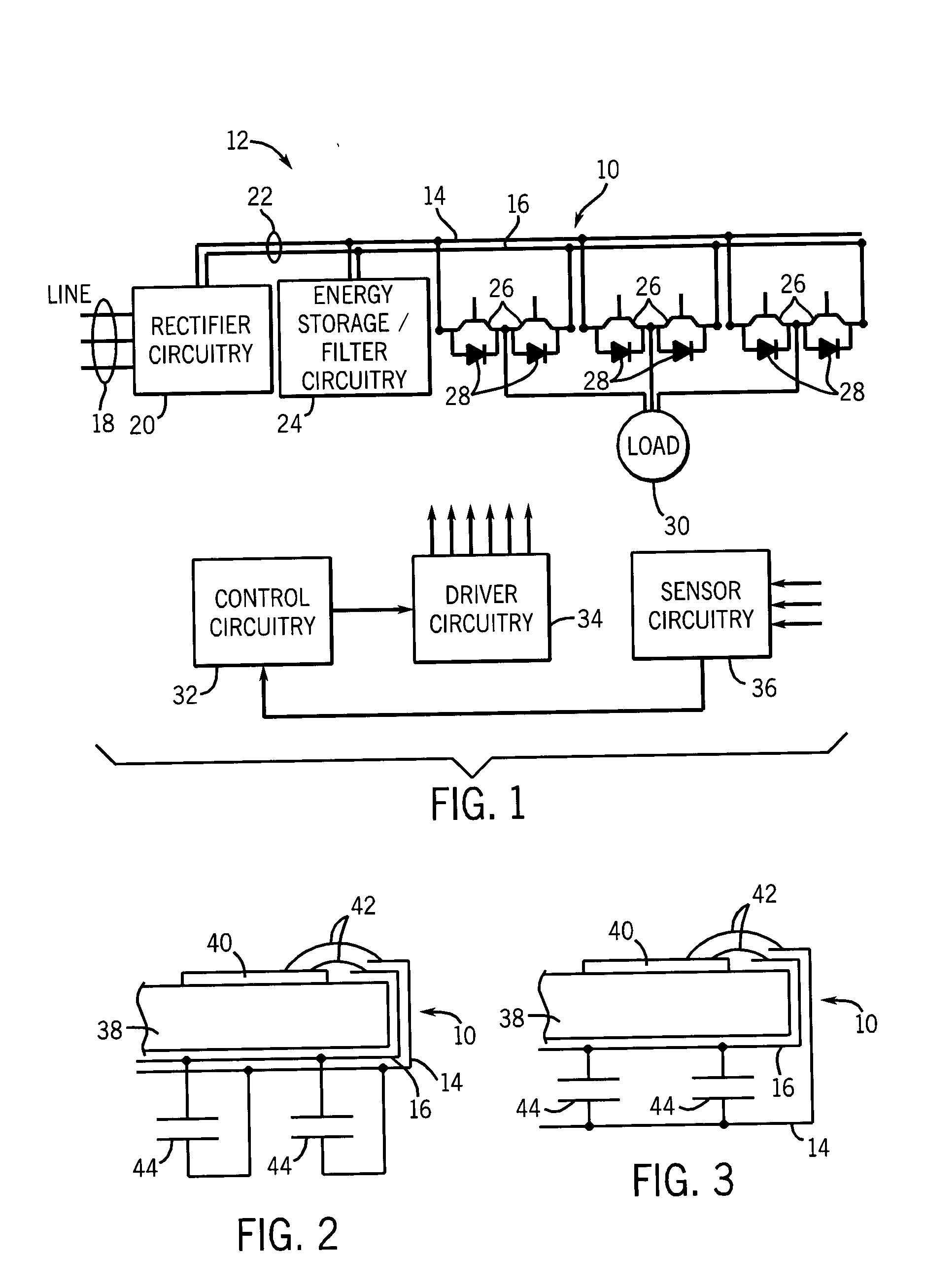
[0017] Turning now to the drawings, and referring first to FIG. 1, a bus system 10 in accordance with the present technique is illustrated diagrammatically as applied to a power converter circuit 12. The bus system includes a pair of bus elements 14 and 16 which extend generally parallel to one another in generally core extensive planes. It should be noted that, as described herein, the bus system is, in exemplary embodiments, comprised of two generally parallel elements. However, additional elements, linked to one another or separate from one another may be provided in the alternative configurations. Similarly, while the elements are generally co-extensive with one another, some degree of non-overlap may occur in the elements, as described more fully below in an exemplary embodiment. Moreover, while the elements are described as extending generally in planes, it should be understood that the elements are planar in so much as they are generally flat. A distinct advantage of the pres...


PUM


Abstract

A bus system is disclosed for use with switching devices, such as power electronic devices. The system includes generally parallel bus elements that define electrical reference planes, such as for a dc bus. The bus elements are separated from one another by insulative layers, with additional insulative layers being available for separating the system from other circuit components. Portions of the bus elements are extended or exposed to permit connection to the circuit elements, including packaged switching circuits and energy storage or filtering circuits. The bus system may be conformed to a variety of geometric configurations, and substantially reduces parasitic inductance and total loop inductance in the resulting circuitry.

Description

BACKGROUND OF THE INVENTION [0001] The present application relates generally to the field of power electronics and power switching devices. More particularly, the invention relates to a novel bus structure for use in such devices to reduce parasitic inductance. [0002] Many applications exist for power electronic devices, including solid state switches. Such applications are found throughout the industry, and increasingly in non-industrial settings as well. In general, solid state switches may be used in a variety of circuitry, such as in inverter circuits that simulate desired waveforms, such as ac waveforms. In industrial drive applications, for example, power may be received from the power grid, converted to dc power, and then reconverted to controlled-frequency ac power by a switched inverter circuit. Devices of this type are used in conventional variable frequency drives, as well as in a variety of other products. Other applications include power converters, generators, power co...

Claims


Application Information

Patent Timeline
IPC IPC(8): G11C7/00H01L25/07H02M7/00
CPCH01L25/072H02M7/003H01L2924/30107H01L2924/3011H01L2924/13055H01L2224/49109H01L2224/48091H01L2924/13091H01L2924/00014H01L2924/00
Inventor RADOSEVICH, LAWRENCE D.KAISHIAN, STEVEN C.KANNENBERG, DANIEL G.ROEBKE, TIMOTHY A.MEYER, ANDREAS A.KEHL, DENNIS L.GETTELFINGER, LEE A.
Owner ROCKWELL AUTOMATION TECH
Why Eureka
Try Eureka