

Method for forming resist pattern and method for manufacturing semiconductor device
a technology of resist film and pattern, which is applied in the direction of photomechanical equipment, photosensitive material processing, instruments, etc., can solve the problems of resist film not having the desired shape, deteriorating image quality,
- Summary
- Abstract
- Description
- Claims
- Application Information
AI Technical Summary
Benefits of technology
Problems solved by technology
Method used
Image

Examples
first embodiment
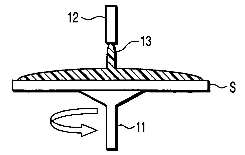
[0032]FIG. 1 is a view showing an apparatus configuration in which a method for forming a resist pattern is implemented. As shown in FIG. 1, a silicon substrate (semiconductor substrate, semiconductor wafer, substrate to be processed) S is arranged below an objective lens 1 disposed in a liquid immersion type exposing apparatus. A space between the objective lens 1 and the silicon substrate S is filled with a liquid (pure water) 2. As described later, a resist film R is formed on the silicon substrate S, and a resist protective film R1 is further formed on a surface of the resist film R.
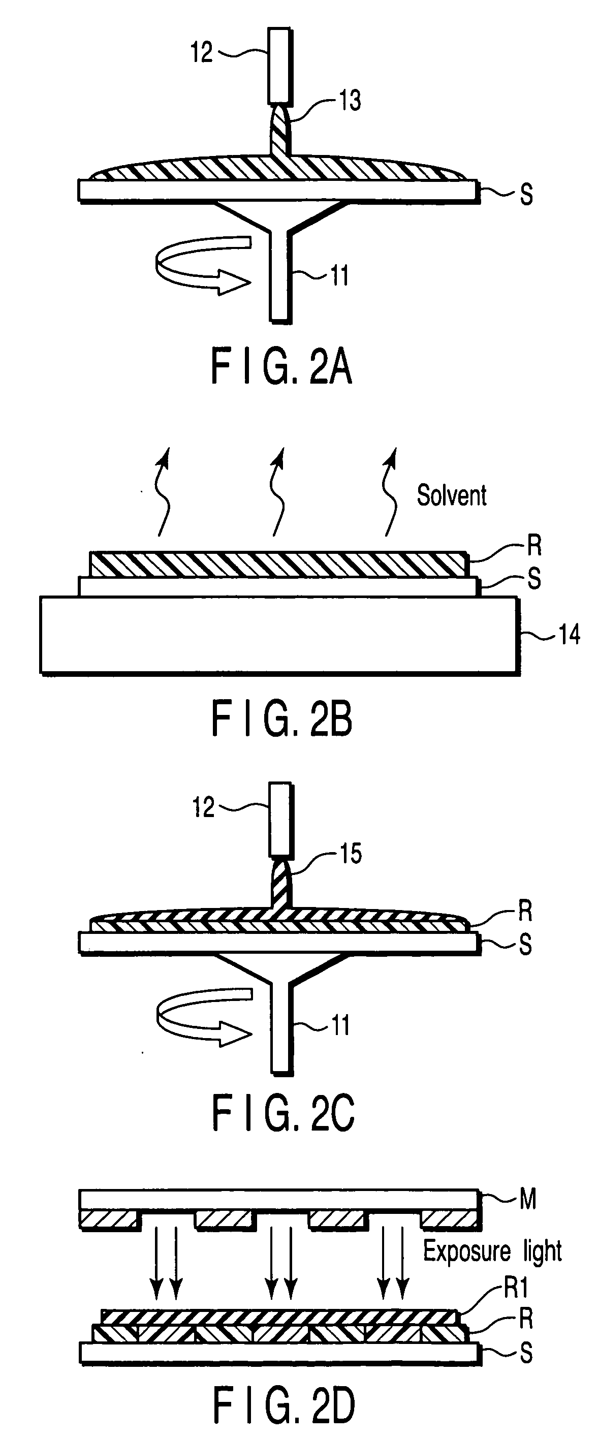
[0033]FIGS. 2A to 2D and FIGS. 3A to 3D are views showing a process flow of the method for forming the resist pattern according to the first embodiment. Hereinafter, the process of the resist pattern formation will be described with reference to FIGS. 2A to 2D and FIGS. 3A to 3D.
[0034] First, a reflection preventing film solution (ARC29A by Nissan Chemical Co. Ltd.) is applied on the silicon substr...
second embodiment
[0041]FIG. 5 is a view showing an apparatus configuration in which a method for forming a resist pattern is implemented. As shown in FIG. 5, a silicon substrate S is arranged below an objective lens 1 disposed in a liquid immersion type exposing apparatus. A space between the objective lens 1 and the silicon substrate S is filled with a liquid (pure water) 2. As described later, a resist film R is formed on the silicon substrate S, and a surface of the resist film R becomes hydrophilic.
[0042]FIGS. 6A to 6D and FIGS. 7A to 7C are views showing a process flow of the method for forming the resist pattern according to the second embodiment. Hereinafter, the process of the resist pattern formation will be described with reference to FIGS. 6A to 6D and FIGS. 7A to 7C.
[0043] First, a reflection preventing film solution (ARC29A by Nissan Chemical Co. Ltd.) is applied on the silicon substrate S, baked on a hot plate at 190° C. for 60 sec., and a reflection preventing film (film to be proce...
third embodiment
[0050]FIGS. 8A to 8D and FIGS. 9A to 9C are views showing a process flow of a method for forming a resist pattern according to a Hereinafter, the process of the resist pattern formation will be described with reference to FIGS. 8A to 8D and FIGS. 9A to 9C.
[0051] First, as in the case of the second embodiment, as shown in FIGS. 8A, 8B, a resist film R is formed on a silicon substrate S. Subsequently, as shown in FIG. 8C, the resist film R is irradiated with an excimer light by a VUV excimer lighting device 18 of 172 nm at a room temperature in the atmosphere for 10 sec. Irradiance is 5 mW / cm2, and a gap between a lamp and the silicon substrate S is 2 mm. Accordingly, a contact angle of the pure water with a surface of the resist film R is reduced from 65° to 35°.
[0052] Next, as shown in FIG. 8D, in a liquid immersion type ArF excimer laser exposing apparatus that uses water as a medium, a line-and-space pattern of a line width 100 nm is transferred through an objective lens 1 to th...
PUM
 Abstract
Description
Claims
Application Information