Method of semiconductor device protection, package of semiconductor device

Inactive Publication Date: 2005-04-07
SOCIONEXT INC
View PDF7 Cites 14 Cited by
  • Summary
  • Abstract
  • Description
  • Claims
  • Application Information

AI Technical Summary

Benefits of technology

[0037] According to the present invention, when packaging a semiconductor device in a tray having a first semi-tray and a second semi-tray, because the semiconductor device is protected by a protection cover between the first semi-tray and a surface of the semiconductor device, it is possible to prevent damage to the semiconductor device during transporta

Problems solved by technology

In a semiconductor device generating a large amount of heat and having high power consumption, the temperature of the built-in semiconductor chip tend to increase, hence after mounting of the semiconductor chip, it is necessary to directly cool the top surface of the chip.
Especially, in the performance tests, when pressing a semiconductor device on a contactor or into a socket, only the chip itself is directly pressed, and this may cause cracks or defects in the chip.
Further, when pressing a number of semiconductor chips at the same time, the load applied on the semiconductor chips may be non-uniform because of unevenness of the surface of the semiconductor device caused by height differences and deviation of mounting positions of the semiconductor chips.
This is the so-called unbalanced load problem.
When unbalanced load occ

Method used


Image

  • Method of semiconductor device protection, package of semiconductor device
  • Method of semiconductor device protection, package of semiconductor device
  • Method of semiconductor device protection, package of semiconductor device

Examples


first embodiment

[0089] First Embodiment

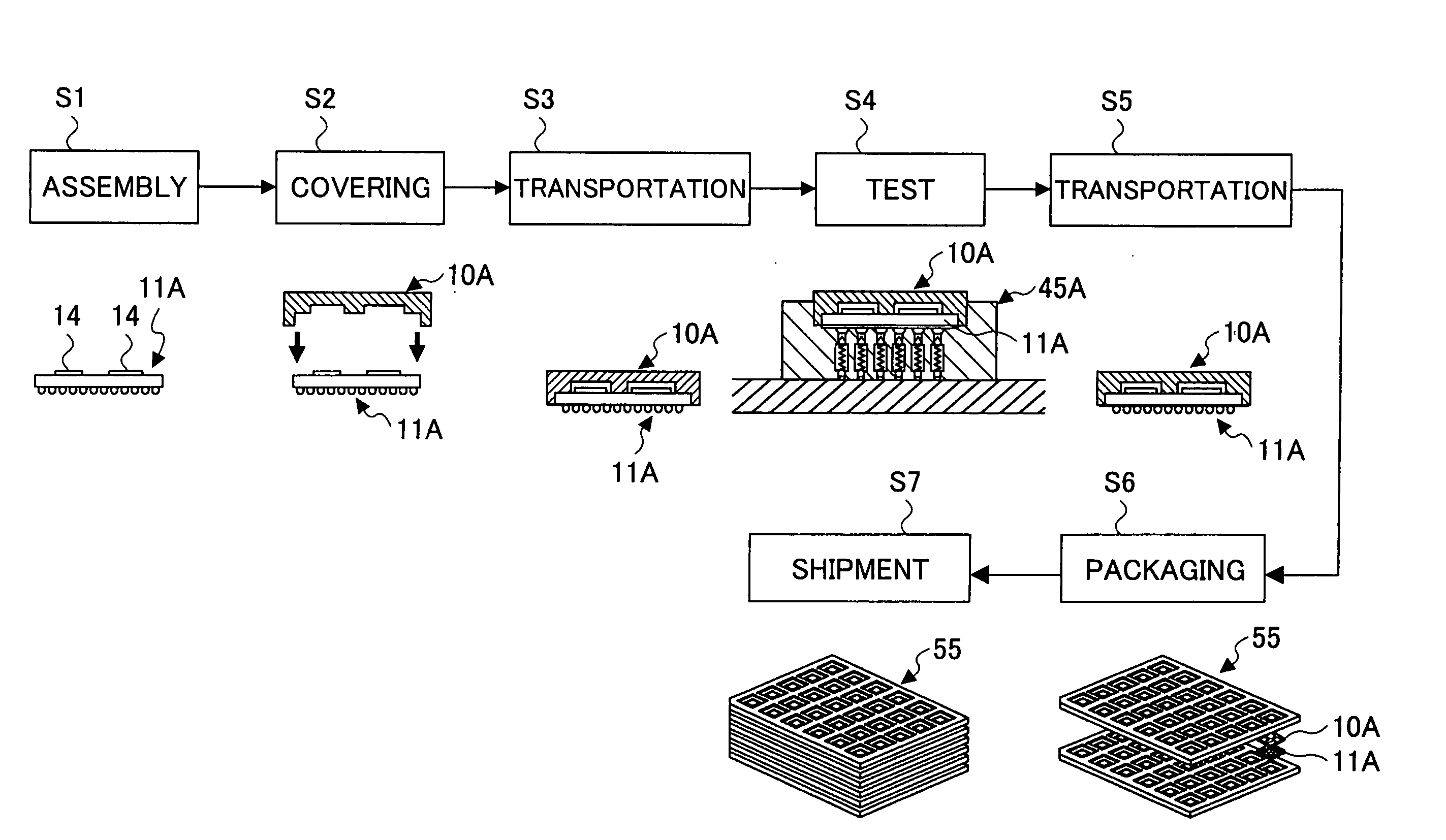
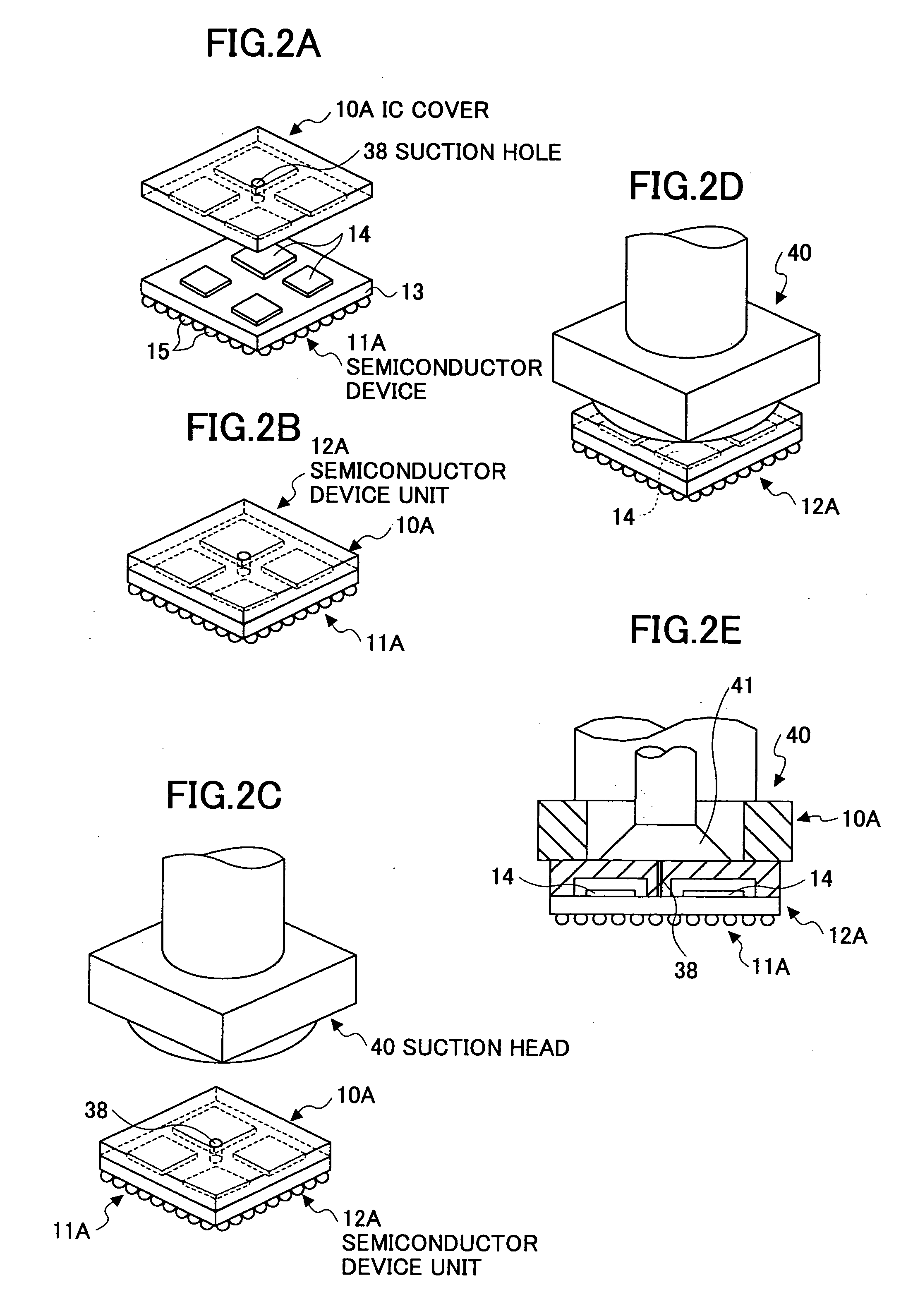
[0090] As described above, in the fabrication and processing steps as shown in FIG. 1, after the semiconductor device 11A is fabricated in step S1, in the subsequent step S2, the IC cover 10A is mounted on the semiconductor device 11A. In the subsequent transportation steps S3 and S5, test step S4, packaging step S6, and shipment step S7, the semiconductor device 11A is processed with the IC cover 10A mounted on the semiconductor device 11A.

[0091] In the present embodiment, the covering step S2 is performed before steps S3 through S7 are executed, but the timing of mounting the IC cover 10A on the semiconductor device 11A is not limited to this. The IC cover 10A can be mounted on the semiconductor device 11A at any stage (for example, between step S3 and step S4) when necessary. However, it is preferable to mount the IC cover 10A on the semiconductor device 11A right after fabrication and before the various treatments from steps S3 to S7, because this can pre...

second embodiment

[0152] Second Embodiment

[0153]FIG. 11 is a perspective view of an IC cover 10B and a semiconductor device 11B according to a second embodiment. In FIG. 11, the same reference numbers are used for the same elements as those shown in the preceding embodiment.

[0154] As shown in FIG. 11, the IC cover 10B is attached to the semiconductor device 11B.

[0155] In the semiconductor device 11B, a semiconductor chip 14 and a number of electric parts 18 (for example, chip condensers) are mounted on a surface 13A of an interposer 13. The semiconductor chip 14 is connected to the interposer 13 by means of flip chip mounting (face down); an under-fill material 17 is provided between the semiconductor chip 14 and the interposer 13 to improve the connection reliability. The under-fill material 17 extends until the peripheral area of the semiconductor chip 14. The electric parts 18 are arranged in proximity of the semiconductor chip 14, to surround the semiconductor chip 14.

[0156] The semiconductor ...

third embodiment

[0159] Third Embodiment

[0160]FIG. 12 is a perspective view of an IC cover 10C and a semiconductor device 11C according to a third embodiment. In FIG. 12, the same reference numbers are used for the same elements as those shown in the preceding embodiments.

[0161] As shown in FIG. 12, the IC cover 10C is attached to the semiconductor device 11C.

[0162] In the semiconductor device 11C, a semiconductor chip 14 and solder balls 19 for stacking are arranged on a surface 13A of an interposer 13.

[0163] The semiconductor device 11C is obtained by stacking other not-illustrated semiconductor devices when mounting the semiconductor device 11C. Therefore, in addition to the solder balls 15 on the lower surface of the interposer 13, the solder balls 19 are also prepared on the upper surface for use in stacking.

[0164] For this reason, on the IC cover 11C attached to the semiconductor device 11C, in addition to a recess 22 in correspondence to the position of the semiconductor chip 14, bump rec...


PUM

PropertyMeasurementUnit
Electrical conductivityaaaaaaaaaa
Shapeaaaaaaaaaa
Elasticityaaaaaaaaaa

Abstract

A method for protecting a semiconductor device is disclosed that can improve reliability of a performance test for the semiconductor device and prevent damage to the semiconductor device during transportation or packaging for shipment. An IC cover is attached to the semiconductor device, which has height unevenness because it includes semiconductor chips and electric parts having different heights. The IC cover includes projecting portions and a base portion. After being attached to the semiconductor device, the projecting portions stand in a free area in the semiconductor device, and the base portion is supported by the projections to be separated from the semiconductor chips and electric parts in the semiconductor device. The IC cover is detachably attached to the semiconductor device.

Description

BACKGROUND OF THE INVENTION [0001] 1. Field of the Invention [0002] The present invention relates to a semiconductor device unit that enables easy transportation, test, or packaging and shipment of a semiconductor device, a packaging structure of the semiconductor device, a semiconductor device protection method, and a protection cover of the semiconductor device. [0003] 2. Description of the Related Art [0004] In the recent years and continuing, because portable devices, such as PDAs (personal digital assistant), mobile phones, and digital cameras are becoming light and small, it is also required that semiconductor devices used in these portable devices be light and small. [0005] In response to this requirement, the so-called “chip size package” (CSP) is rapidly spreading, which further reduces package size close to the size of the packaged semiconductor element (chip). [0006] Typical examples of CSP include FBGA (Fine-pitch Ball Array), FLGA (Fine-pitch Land Grid Array). [0007] In...

Claims


Application Information

Patent Timeline
IPC IPC(8): H01L21/50G01R31/26H01L21/66H01L21/673H01L23/00H01L23/04H01L23/544H01L23/58
CPCH01L21/50Y10T29/49826H01L22/20H01L23/04H01L23/544H01L25/0655H01L2223/54473H01L2924/014H01L2924/15311H01L2924/16153H01L2924/1616H01L2924/166H01L2924/0002H01L21/67333H01L2924/00
Inventor TASHIRO, KAZUHIROFUKUDA, KEISUKEKOHASHI, NAOHITOMARUYAMA, SHIGEYUKI
Owner SOCIONEXT INC
Why Eureka
Try Eureka