Solid state image sensor

a solid-state image and sensor technology, applied in the field of image sensors, can solve the problems of reducing the ability of the pixel to collect photon-generated electrons, and severely reducing sensitivity

Active Publication Date: 2005-04-07
STMICROELECTRONICS RES & DEV
View PDF6 Cites 17 Cited by
  • Summary
  • Abstract
  • Description
  • Claims
  • Application Information

AI Technical Summary

Problems solved by technology

However, these layouts have a disadvantage in that the additional circuitry in each pixel severely reduc

Method used


Image

  • Solid state image sensor
  • Solid state image sensor
  • Solid state image sensor

Examples


Embodiment Construction

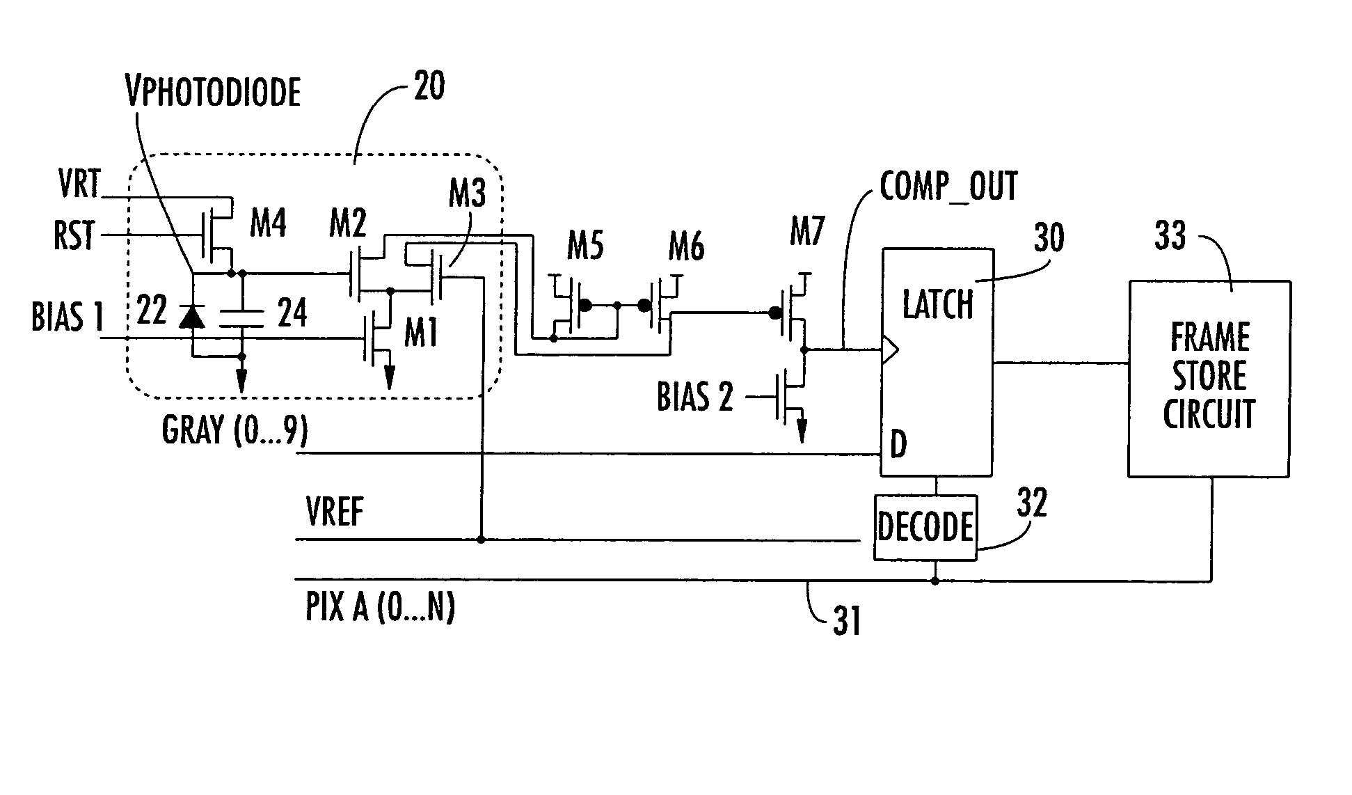
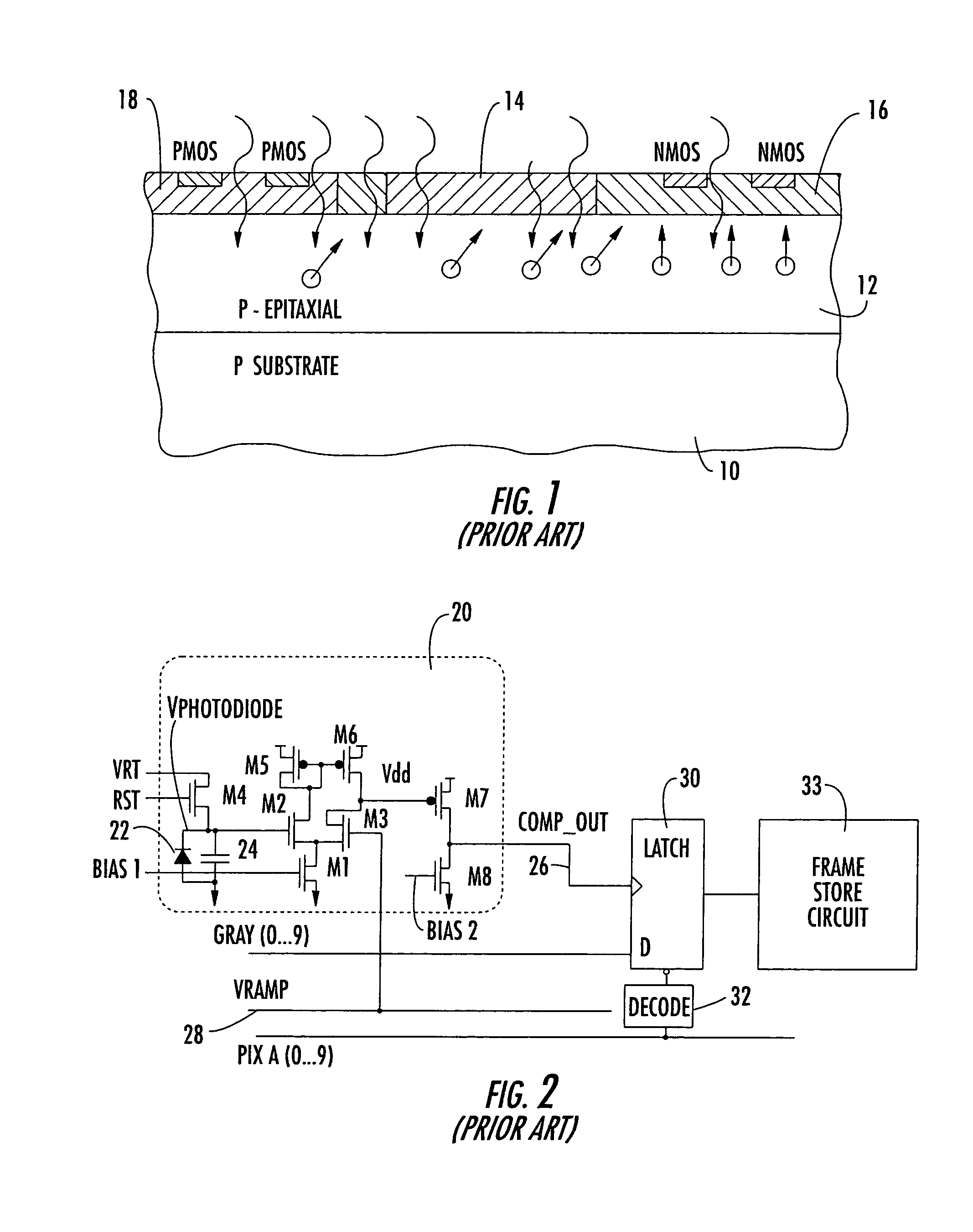
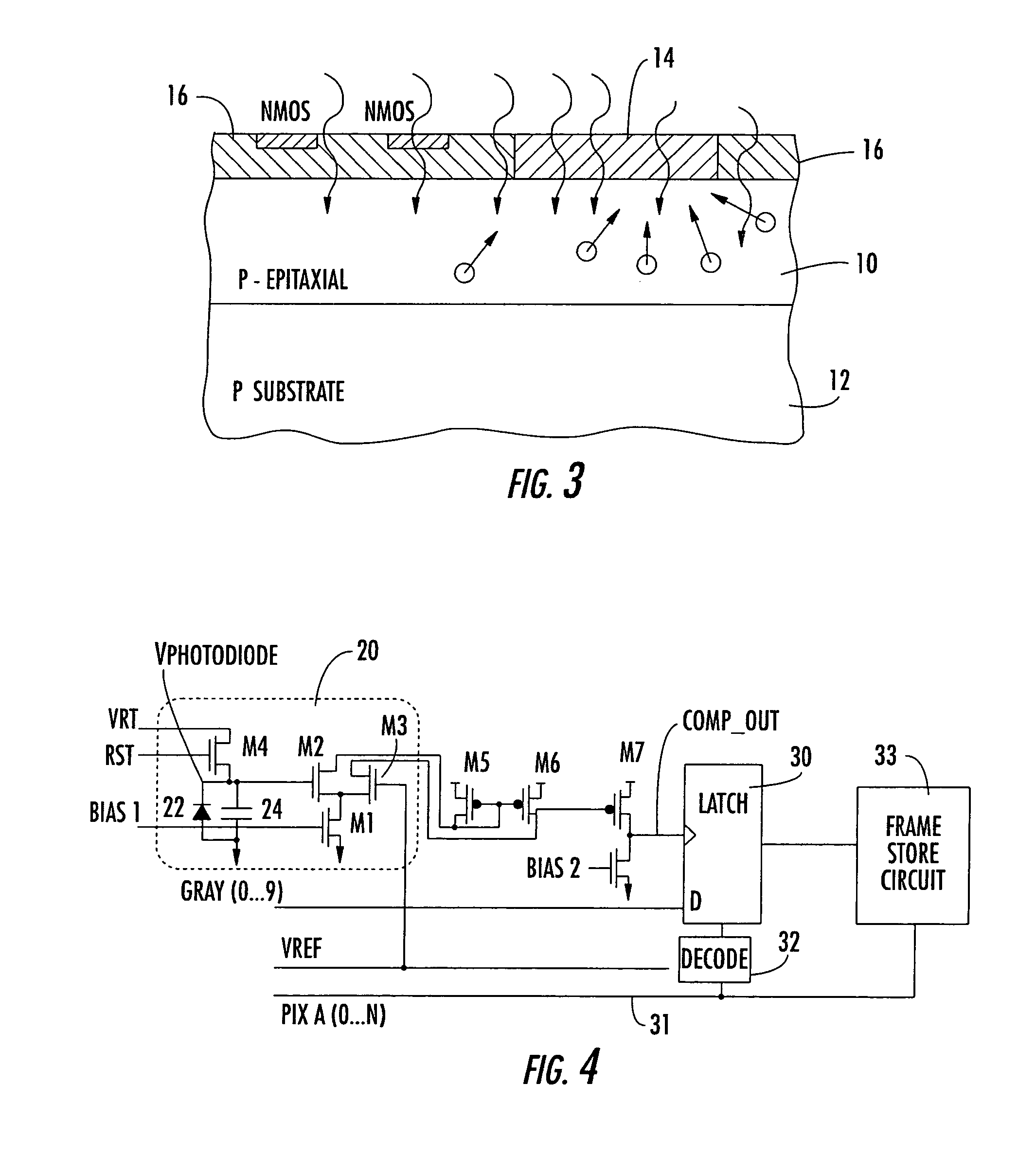
[0018]FIG. 1 shows a prior art approach to an image sensor having in-pixel circuitry such as an A-D converter. The sensor is formed on a P-type epitaxial layer 12 overlying a P-type substrate 10. The top part of the P-type epitaxial layer 12 is doped to provide the circuit components, namely an N-well 14 forming a collection node, NMOS transistors in a P-well 16, and PMOS transistors in an N-well 18.

[0019] For correct operation, the P-well 16 is biased to Vss (ground / 0V), and the N-well is biased to Vdd, typically 3.3V or 1.8V. The collection node 14 is biased to a voltage between Vss and Vdd.

[0020] Light is absorbed by the silicon at a depth which is wavelength dependent. Typically, visible light generates a substantial number of electrons at a depth that is greater than the wells 14, 16 and 18. The collection node 14 as shown in FIG. 1 will collect electrons that are generated directly beneath it. The electrons which are generated close to the border of the collection node 14 an...


PUM


Abstract

An active pixel image sensor is formed on a P-type epitaxial layer on a P-type substrate. An active pixel array is in the P-type epitaxial layer. Each pixel includes an N-well functioning as a collection node, and a P-well adjacent the N-well. The P-well includes only NMOS transistors functioning as active elements. The in-pixel transistors cooperate with off-pixel PMOS transistors to form A-D converters.

Description

FIELD OF THE INVENTION [0001] The present invention relates to image sensors, and in particular, to solid state image sensors with active pixels. BACKGROUND OF THE INVENTION [0002] As is well known, in active pixel image sensors an area of the pixel acts as a photodiode, with photon-generated current being integrated on the self-capacitance of the photodiode. This charge is essentially an analog representation of light received at that pixel during the exposure period. When a digital signal is desired, it is necessary to provide A-D conversion. [0003] Most active pixels use one or more A-D converters located off the image plane. This maximizes the light-converting properties of the image plane, but at the expense of requiring a relatively complex switching or multiplexing arrangement to transfer pixel signal values to the A-D converters. [0004] Layouts have been proposed in which each pixel has its own A-D converter; see for example U.S. Pat. Nos. 5,461,425 and 5,801,657 to Fowler e...

Claims


Application Information

Patent Timeline
IPC IPC(8): H01L27/146H04N3/15
CPCH04N3/155H01L27/14609H04N25/772
Inventor RAYNOR, JEFF
Owner STMICROELECTRONICS RES & DEV
Why Eureka
Try Eureka