CMOS image sensor and manufacturing method thereof

a technology of image sensor and manufacturing method, which is applied in the direction of diodes, radiation control devices, semiconductor devices, etc., can solve the problems of damage to the photodiode b>106/b>, and achieve the effect of efficiently transferring the potential variation of the photodiod

Inactive Publication Date: 2005-04-07
DONGBU HITEK CO LTD
View PDF24 Cites 8 Cited by
  • Summary
  • Abstract
  • Description
  • Claims
  • Application Information

AI Technical Summary

Benefits of technology

[0011] The present invention has been made in an effort to solve the above problems, and to provide a CMOS image sensor which is capable of efficiently transferring the potential variation of the photodiode to an adjacent gate terminal.

Problems solved by technology

Conventional CMOS image sensors such as CMOS image sensor 100 have a drawback in that photodiode 106 may be damaged when contact hole 116 is formed by a dry etching technique.

Method used


Image

  • CMOS image sensor and manufacturing method thereof
  • CMOS image sensor and manufacturing method thereof
  • CMOS image sensor and manufacturing method thereof

Examples


Embodiment Construction

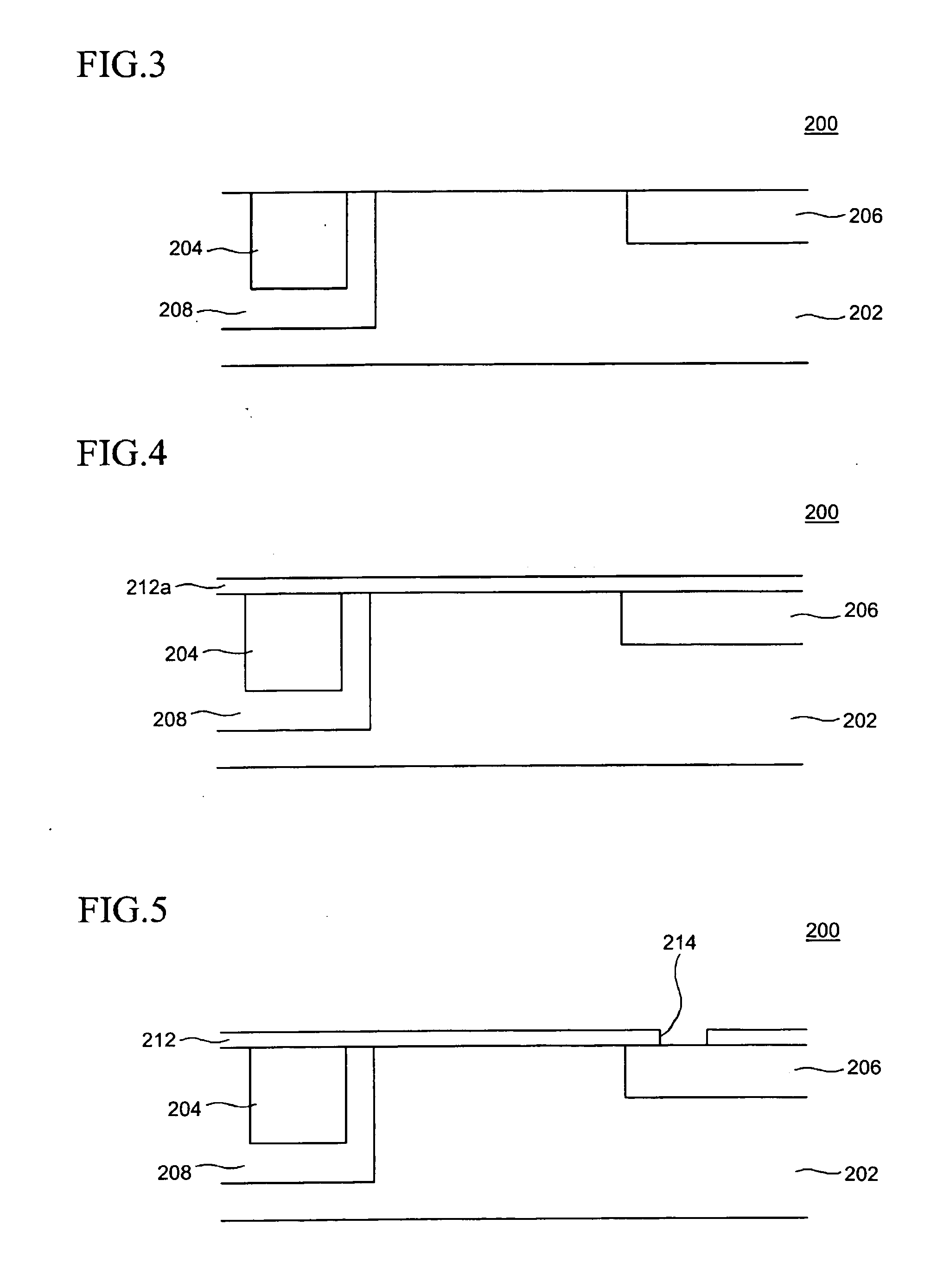
[0020] Reference will now be made in detail to the present embodiments of the invention, examples of which are illustrated in the accompanying drawings. Wherever possible, the same reference numbers will be used throughout the drawings to refer to the same or like parts. In the drawings, the thickness of layers, films and regions are exaggerated for clarity.

[0021] A CMOS image sensor and a manufacturing method thereof consistent with an embodiment of the present invention will be described with reference to FIGS. 1-6 in detail.

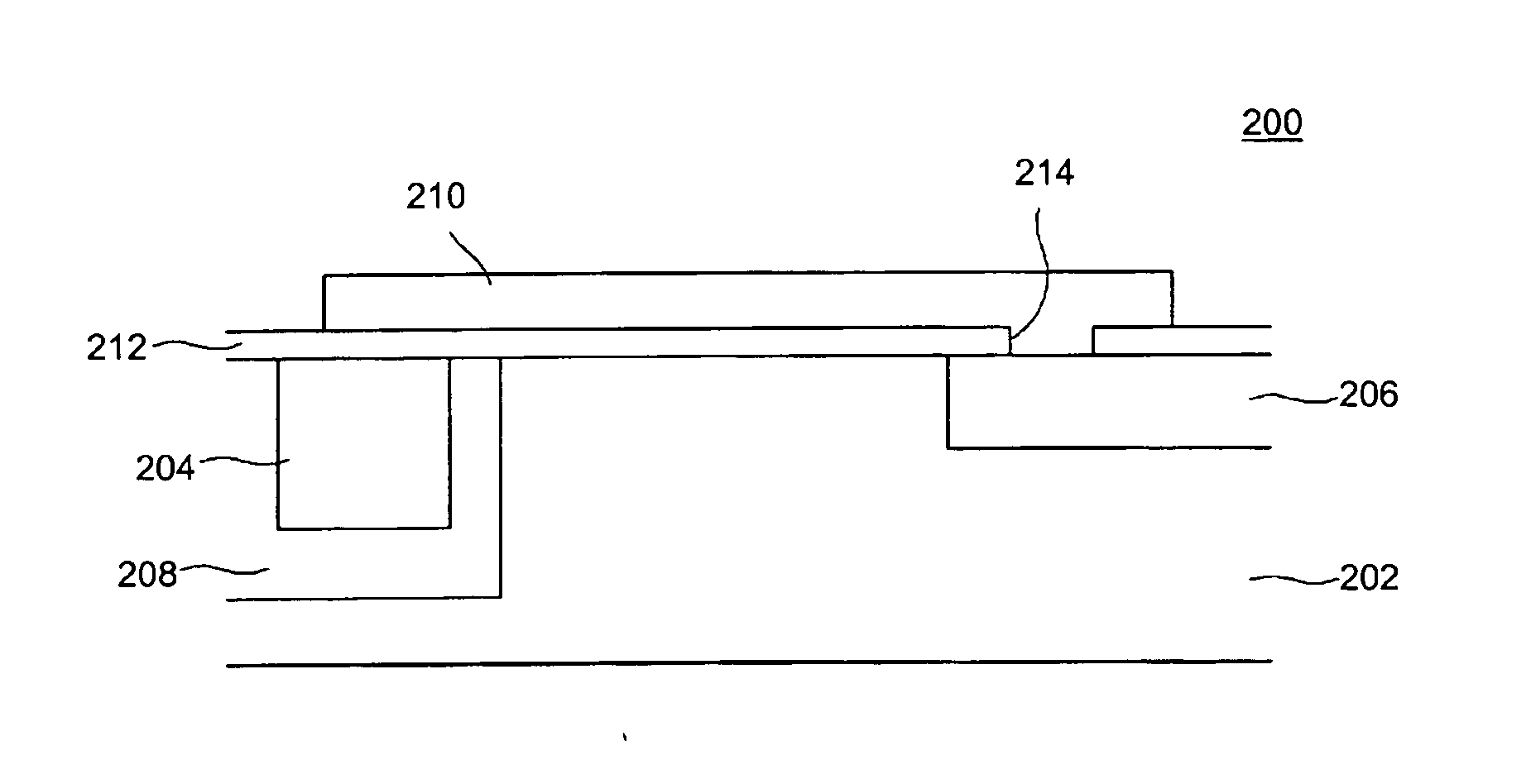
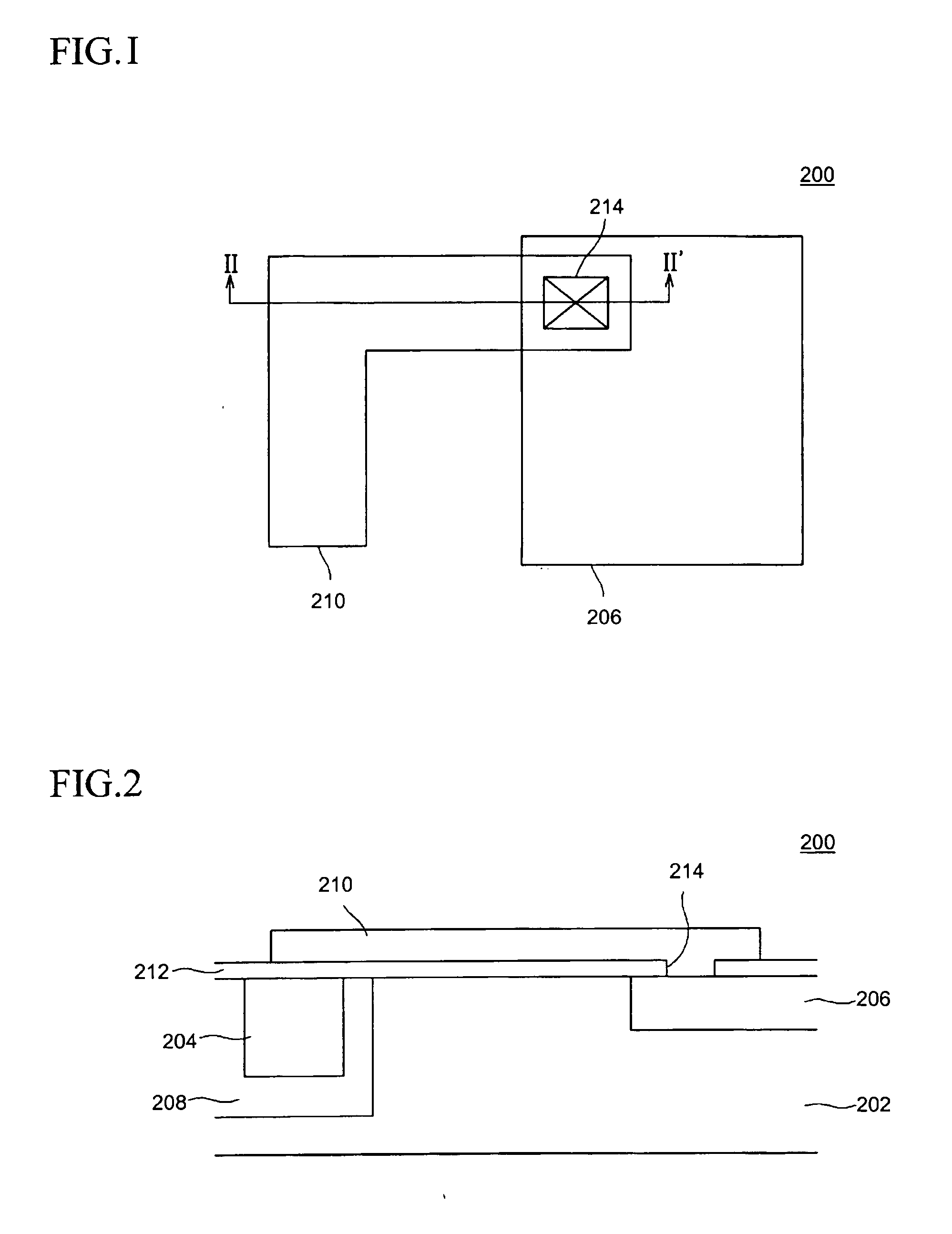
[0022] A CMOS image sensor generally includes a pixel array structure comprised of a plurality of unit pixels. Each unit pixel may comprise a plurality of transistors and a photodiode. In one aspect, each unit pixel includes three transistors and one photodiode.

[0023] In one aspect, the photodiode of the CMOS image sensor comprises polysilicon and is connected to a gate terminal of an adjacent MOS transistor of the CMOS image sensor. Consistent with an embo...


PUM


Abstract

A CMOS image sensor-manufacturing method includes forming a photodiode on a substrate, forming an insulating layer over the substrate, forming a contact hole in the insulating layer, and forming a gate terminal over the insulating layer. The gate terminal is connected to the photodiode through the contact hole.

Description

RELATED APPLICATION [0001] This application is related to and claims priority under 35 U.S.C. § 119 to Korean Patent Application No. 10-2003-0068497, filed on Oct. 1, 2003, the entire contents of which are expressly incorporated herein by reference. BACKGROUND [0002] (a) Technical Field [0003] The present invention relates to a CMOS image sensor and a manufacturing method thereof. [0004] (b) Description of Related Art [0005] A semiconductor image sensor is a semiconductor device converting optical images into electrical signals and typically manufactured in a type of a charge coupled device (CCD) or a complementary metal oxide semiconductor (CMOS) image sensor. [0006] A charge coupled device is an integrated circuit containing an array coupled capacitors. Each capacitor stores and transfers electric charges to one or more of the neighboring capacitors thereof. [0007] In contrast, a CMOS image sensor includes MOS transistors, photo-sensing regions for detecting an external light and ...

Claims


Application Information

Patent Timeline
Patent Type & Authority Applications(United States)
IPC IPC(8): H01L21/00H01L27/146H01L31/062
CPCH01L27/1463H01L27/14689H01L27/14643H01L27/146
Inventor JEON, IN-GYUN
Owner DONGBU HITEK CO LTD
Why Eureka
Try Eureka