Prestage for an off-chip driver (OCD)

a technology of off-chip drivers and prestages, which is applied in the field of prestages of off-chip drivers, can solve the problems of insensitivity of data, deceleration of switch edges through on-chip voltage drops on the on-chip supply voltage lines, and data eye corruption by several undesirable mechanisms, so as to achieve low circuit complexity of integrated circuits and achieve low cost. , the effect of lowering the cos

Inactive Publication Date: 2006-04-13
POLARIS INNOVATIONS
View PDF3 Cites 2 Cited by
  • Summary
  • Abstract
  • Description
  • Claims
  • Application Information

AI Technical Summary

Benefits of technology

[0028] Analogously, it is advantageous to connect the base terminal of the current source to a base potential, which is more positive than the supply potential, when it is required that the prestage supplies (i.e. delivers) a constant predetermined current at its output during switching. In such a case, it is effective to connect the second supply terminal of the circuitry to the reference potential for generating an output signal.
[0029] In a preferred embodiment of the present invention, the prestage comprises a charge pump for generating the base potential. Such an embodiment offers the advantage that no base potential that is more negative than the reference potential or more positive than the supply potential has to be provided to the prestage from the outside.
[0030] On the other hand, it is very advantageous when the prestage is designed to receive the base potential from an external base voltage source. In that case, the circuit complexity for realizing the prestage is very low. An existing prior art circuitry merely has to be changed by providing an additional trace for the base potential as well as terminal for the base potential. This allows again a simple implementation of an inventive prestage in an existing circuit design. Here, the base voltage source can be both outside an integrated circuitry as well as inside an integrated circuitry. Thus, both the supply of an external supply voltage and the generation in an integrated circuitry is possible. Here, the supply of an external base voltage has the advantage that the circuit complexity within the integrated circuit is low. Any base voltage can be provided, which is highly loadable with external provision and not subject to the variations of the reference potential. On the other hand, it is sometimes advantageous to generate the base potential within the integrated circuitry. This is particularly advantageous when it is not possible to provide an integrated circuitry with an additional terminal for supplying a base potential according to existing specifications or standards, respectively. The number of pins does not increase during generation of the base voltage on the integrated circuit which contributes to lowering the costs. Further, nowadays, it is to integrate charge pumps into integrated circuits possible with little effort. In many cases, the required charge pumps are even an integral part of an integrated circuit. In such a case, it is particularly advantageous to use a charge pump already existing in an integrated circuit also for supplying the current sources in the output driver.
[0031] It is particularly advantageous when the prestage is integrated on a chip with integrated circuitry. Such an arrangement provides low production costs as well as good signal quality. Driver prestage, output driver and the integrated circuitry are on a chip, so that no external connections between the same are required. Thus, the signal quality is not decreased. Potentials that are possibly present on the chip can possibly be used as base potential. Thus, the full integration of integrated circuitry and prestage, and, if necessary, also the full output driver, represents both economically and technically...

Problems solved by technology

The data eye can be corrupted by several undesirable mechanisms.
If, for example, all data have the same switching direction, i.e. a low high transition, this results in decelerated switch edges through on-chip voltage drops on the on-chip supply voltage lines.
This increases the precision of the edge steepness at the output of the off-chip driver and thus contributes to an insensitivity of the data eye against interferences.
This reduces the gate potential of the pMOS field-effect transistor.
Thus, it is neither required nor desirable to charge-reverse the gate capacitance any further.
However, it can happen that the control potential at the data input 360 of the p prestage 310 is not sufficiently high.
Unavoidable ohmic voltage drops, which can further be added by ...

Method used


Image

  • Prestage for an off-chip driver (OCD)
  • Prestage for an off-chip driver (OCD)
  • Prestage for an off-chip driver (OCD)

Examples


first embodiment

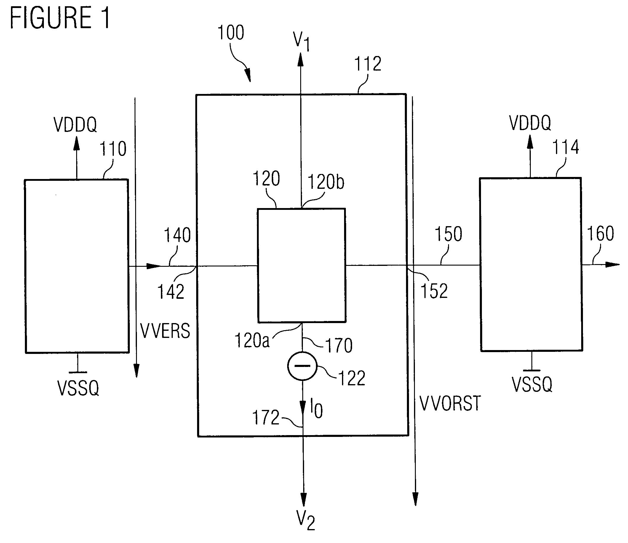
[0038]FIG. 1 shows a block diagram of an inventive circuitry according to the present invention. The circuitry is designated by 100 in its entirety. The circuitry comprises an integrated circuit 110, a prestage 112 as well as an output driver 114. The integrated circuit 110 is connected to a reference potential VSSQ as well as a positive supply potential VDDQ. The potential difference between the supply potential VDDQ and the reference potential VSSQ forms the supply voltage VVERS. The prestage 112 comprises a circuitry 120 for generating an output signal with a first supply voltage terminal 120a and a second supply voltage terminal 120b as well as current source 122 with a current source output 170 and a base terminal 172. The circuitry 120 as well as the current source 122 are connected in series between a first potential V1 and a second potential V2. The potential difference between the first potential V1 and the second potential V2 forms the prestage supply voltage VVORST. Furth...

second embodiment

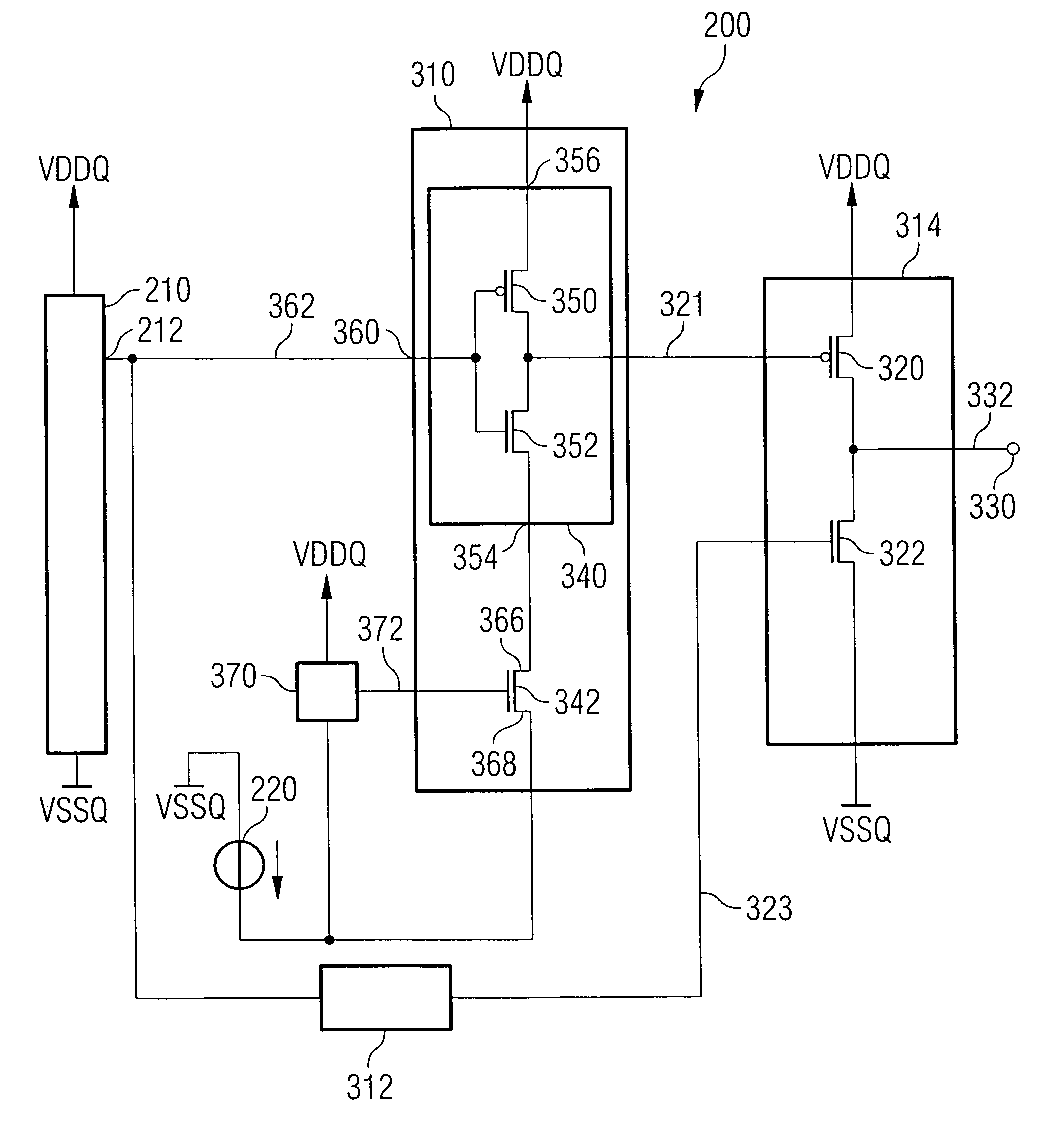
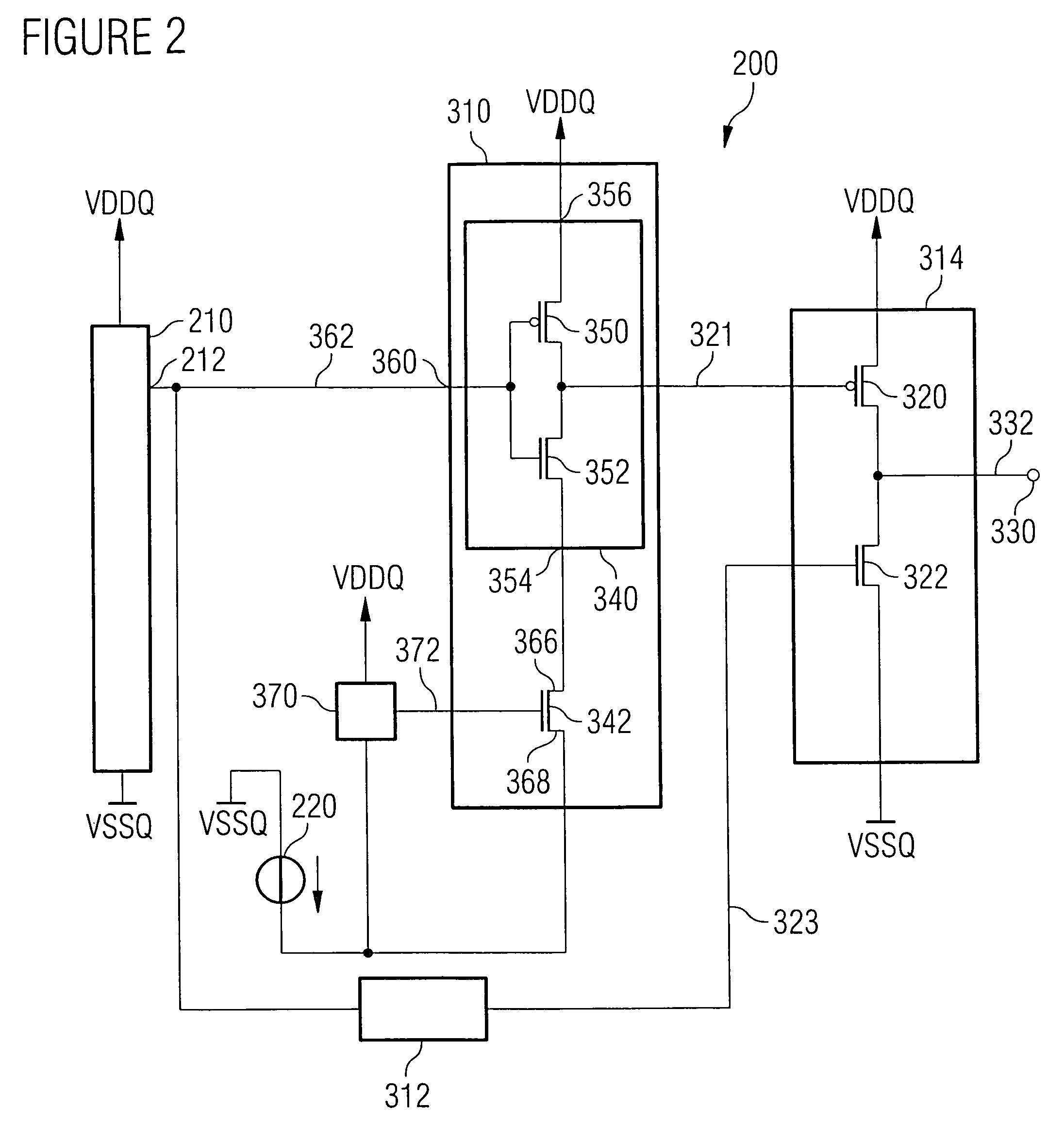
[0041]FIG. 2 shows a portion of a circuit diagram of an inventive circuitry according to the present invention. The circuitry is designated by 200 in its entirety. With regard to structure and mode of operation, the circuitry 200 corresponds mostly to the circuitry 300 according to the prior art described with regard to FIG. 3, so that unaltered parts are not described here. Rather, reference is made to the description of the circuitry 300. Otherwise, the same reference numbers in FIGS. 2 and 3 designate the same means.

[0042] It is the object of the illustrated circuitry to output a signal of an integrated circuit 210 at an external terminal 330. Apart from the means already described above, the circuitry 200 also has an integrated circuit 210, from whose output 212 the prestage input signal 362 is provided. Further, the source terminal of the current source transistor, which is also referred to as base terminal 368, is connected to a base potential VSSV, in contrary to conventional...


PUM


Abstract

A prestage for generating a control signal for an output driver of an integrated circuit, wherein the integrated circuit can be provided with a reference potential and a supply potential fixed in relation to the reference potential, comprises an input for receiving an input signal from the integrated circuit, a circuitry for generating an output signal based on the received input signal, an output for outputting the generated output signals as control signal for an output driver as well as a current source, which is effectively connected to the circuitry. Thereby, the circuitry for generating an output signal and the current source are connected in series and connected to a first potential and a second potential such that a prestage potential difference across the series circuit is higher than a supply potential difference between the supply potential and the reference potential. Such a prestage has the advantage that it is less sensitive against variations on the reference potential or the reference potential, respectively, than conventional circuitries and can generate an output signal with well defined rise times.

Description

[0001] This application claims priority from German Patent Application No. 10 2004 049 194.1, which was filed on Oct. 8, 2004 and is incorporated herein by reference in its entirety. TECHNICAL FIELD [0002] The present invention relates generally to a prestage of an off-chip driver (OCD) of an integrated circuit, particularly to a prestage of an off-chip driver (OCD) for a CMOS memory device (DRAM) with high data rate. BACKGROUND [0003] In memory devices, such as dynamic memory devices with read and write access (DRAM), the communication of the memory to the external world is performed with the help of receivers and off-chip drivers (off chip drivers=OCD). The receivers receive the data during the write process, while the off-chip drivers (OCDs) provide the read data to the outside world. With the current strongly increasing data rates, the performance of the off-chip driver (OCD) is increasingly important. Thus, the length of a valid read date in a memory device according to the DDR...

Claims


Application Information

Patent Timeline
IPC IPC(8): H03K19/0175
CPCG11C7/1051G11C7/1057G11C11/4093H03K19/00384H03K19/018521
Inventor BRUCKE, PAULFISCHER, HELMUT
Owner POLARIS INNOVATIONS
Why Eureka
Try Eureka