Method of forming poly-silicon thin film transistors
a thin film transistor and polysilicon technology, applied in the direction of transistors, semiconductor devices, electrical equipment, etc., can solve the problems of low product yield, high process cost, complex process, etc., and achieve the effect of reducing the cost of adding driver circuits, good electrical performance, and superiority of a-si tft fabrication
- Summary
- Abstract
- Description
- Claims
- Application Information
AI Technical Summary
Benefits of technology
Problems solved by technology
Method used
Image

Examples
embodiment 1
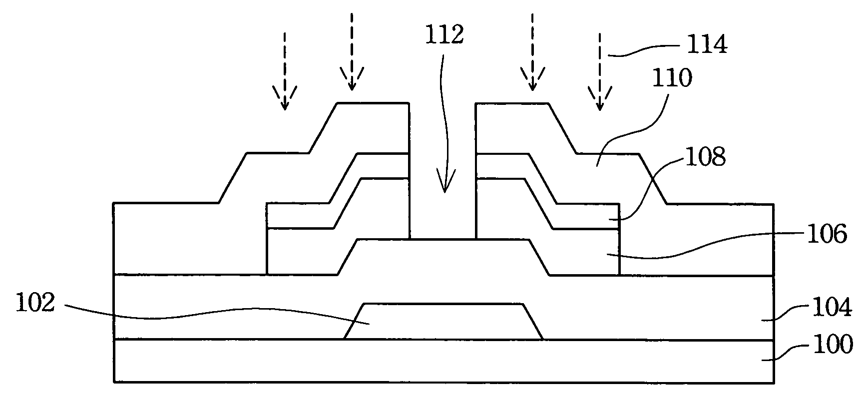
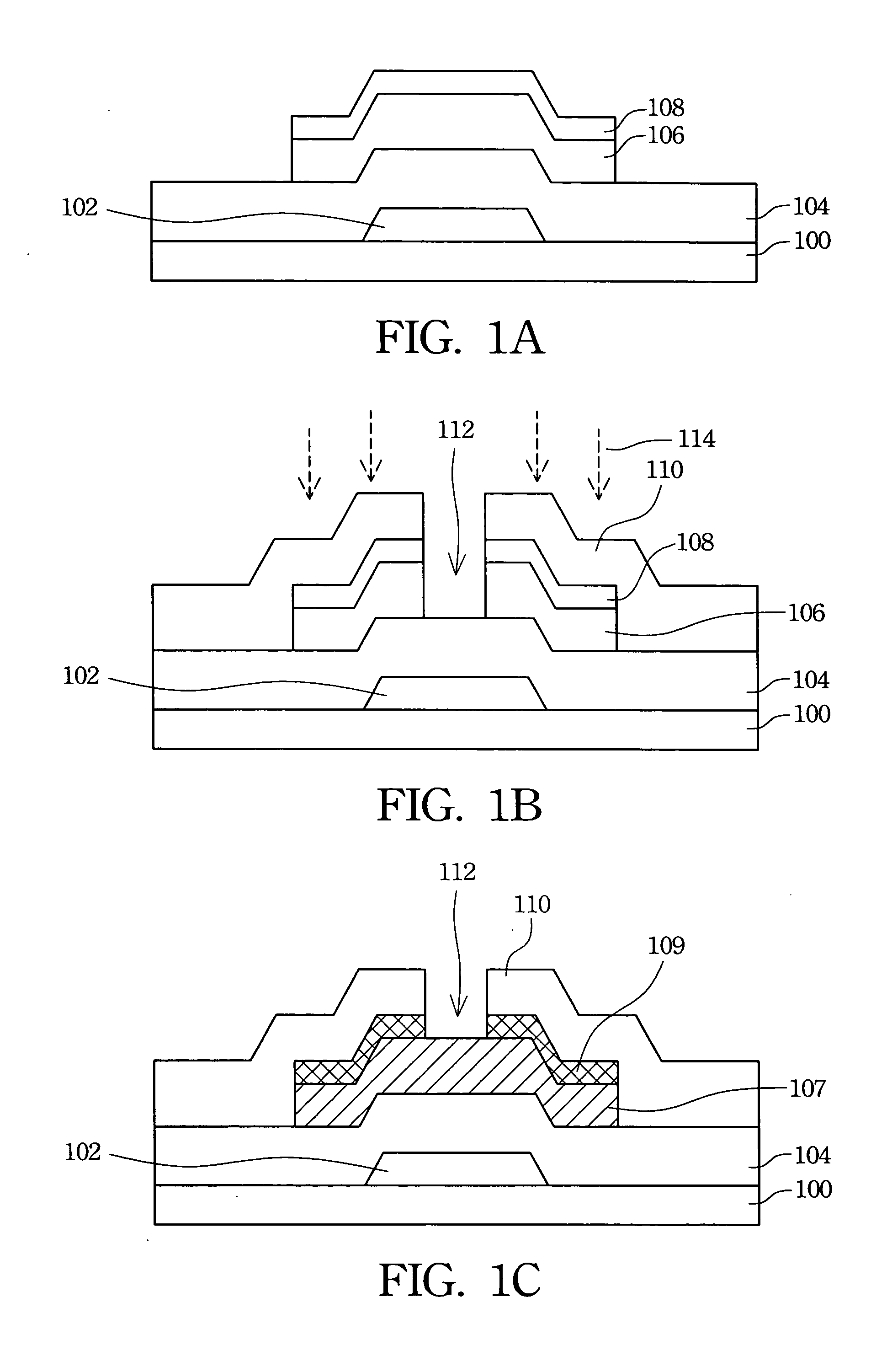
[0019] The present invention discloses a method of forming the poly-Si TFT combined with the bottom-gate BCE structural type. Referring to FIG. 1A, a gate metal 102 is first formed on a substrate 100 by, for example, physical vapor deposition (PVD), and is then patterned by, for example, photolithography and etching. The substrate 100 may be a glass substrate, and the gate metal 102 is a material with good electric conductivity such as chromium (Cr), molybdenum (Mo) or moly-tungsten (MoW), and the gate metal 102 is also a material with good IR absorption and thermal stability.
[0020] A gate insulator 104, an amorphous silicon (a-Si) layer 106, and a doped a-Si layer 108 are formed in turn on the gate metal 102 and the substrate 100 simultaneously by, for example, plasma enhanced chemical vapor deposition (PECVD), and the preferred material of the gate insulator 104 is silicon nitride (SiNx) or silicon oxide (SiOx). Then, the a-Si layer 106 and the doped a-Si layer 108 are patterned ...
embodiment 2
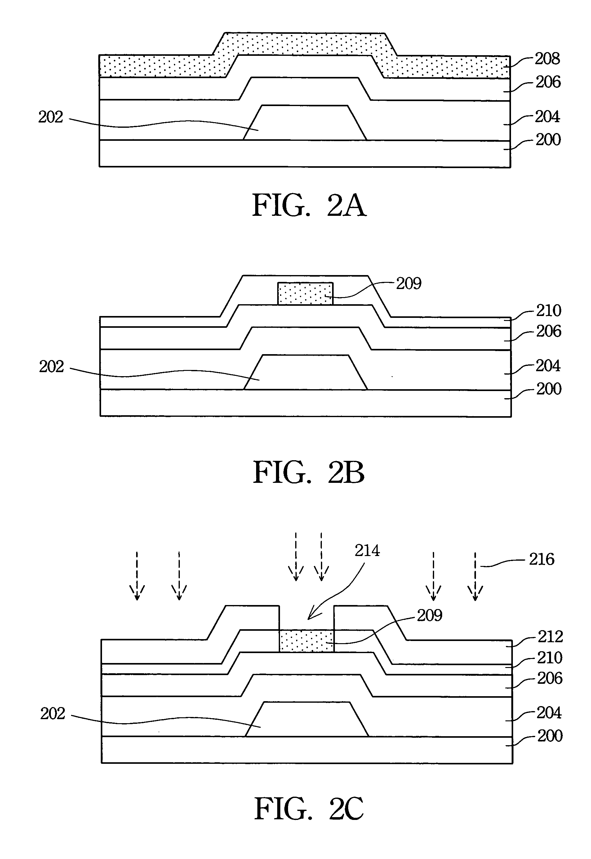
[0025] The present invention discloses another method of forming the poly-Si TFT combined with the bottom-gate CHP structural type. Referring to FIG. 2A, a gate metal 202 is first formed on a substrate 200 by, for example, PVD, and is then patterned by, for example, photolithography and etching. The substrate 200 may be a glass substrate, and the gate metal 202 is a material with good electric conductivity such as Cr, Mo or MoW; the gate metal 202 is also a material with good IR absorption and thermal stability.
[0026] A gate insulator 204, an a-Si layer 206, and a protective layer 208 are formed in turn on the gate metal 202 and the substrate 200 simultaneously by, for example, PECVD, and the preferred material of the gate insulator 204 and the protective layer 208 is SiNx or SiOx.
[0027] Referring to FIG. 2B, the protective layer 208 is patterned by, for example, photolithography and etching to form an etching stop layer 209 for protecting the channel region. Then, a doped a-Si la...
embodiment 3
[0031] The present invention discloses further another method of forming the poly-Si TFT combined with the top-gate structural type. Referring to FIG. 3A, a buffer layer 302 is first formed on a substrate 300 by, for example, PECVD. The substrate 300 may be a glass substrate, and the buffer layer 302 may be a SiOx layer. Then, an a-Si layer 304 is formed on the buffer layer 302 by, for example, PECVD.
[0032] Next, a gate insulator 306 is formed on the a-Si layer 304 by, for example, PECVD; the preferred material of the gate insulator 306 is SiOx. A gate metal 308 is formed by, for example, PVD, and is then patterned by, for example, photolithography and etching. The gate metal 308 is a material with good electric conductivity such as Cr, Mo or MoW, and the gate metal 308 is also a material with good IR absorption and thermal stability.
[0033] Then, referring to FIG. 3B, an ion-implantation is performed, with the gate metal 308 serving as a mask, and the a-Si layer 304 on two sides o...
PUM
 Abstract
Description
Claims
Application Information
 - R&D Engineer
- R&D Manager
- IP Professional
- Industry Leading Data Capabilities
- Powerful AI technology
- Patent DNA Extraction
Browse by: Latest US Patents, China's latest patents, Technical Efficacy Thesaurus, Application Domain, Technology Topic.
© 2024 PatSnap. All rights reserved.Legal|Privacy policy|Modern Slavery Act Transparency Statement|Sitemap