
Relaxed SiGe platform for high speed CMOS electronics and high speed analog circuits

a technology of analog circuits and sige platforms, applied in the direction of semiconductors, electrical devices, transistors, etc., can solve the problems of serious economic and technological problems that will confront the progress of digital integrated circuits, new bottlenecks in data flow, and analog circuitry has barely advanced at all, so as to achieve the effect of minimal surface roughness

Inactive Publication Date: 2005-04-14
TAIWAN SEMICON MFG CO LTD
View PDF99 Cites 132 Cited by
  • Summary
  • Abstract
  • Description
  • Claims
  • Application Information

AI Technical Summary

Benefits of technology

The invention provides a way to make a smooth surface for device layers in a material platform called planarized relaxed SiGe. This platform can be used to make both digital and analog circuits, allowing for the fabrication of high-performance chips that can have both digital and analog functions all in one.

Problems solved by technology

However, new bottlenecks in data flow are appearing as the interconnection hierarchy is expanded.
Although digital integrated circuits have progressed at unprecedented rates, analog circuitry has hardly progressed at all.
Furthermore, it appears that in the near future, serious economic and technological issues will confront the progress of digital integrated circuits.
First, placing Si in tension increases the mobility of electrons moving parallel to the surface of the wafer, thus increasing the frequency of operation of the MOSFET and the associated circuit.
Unfortunately, these devices possess a variety of problems with respect to commercialization.
First, the material quality that is generally available is insufficient for practical utilization, since the surface of SiGe on Si becomes very rough as the material is relaxed via dislocation introduction.
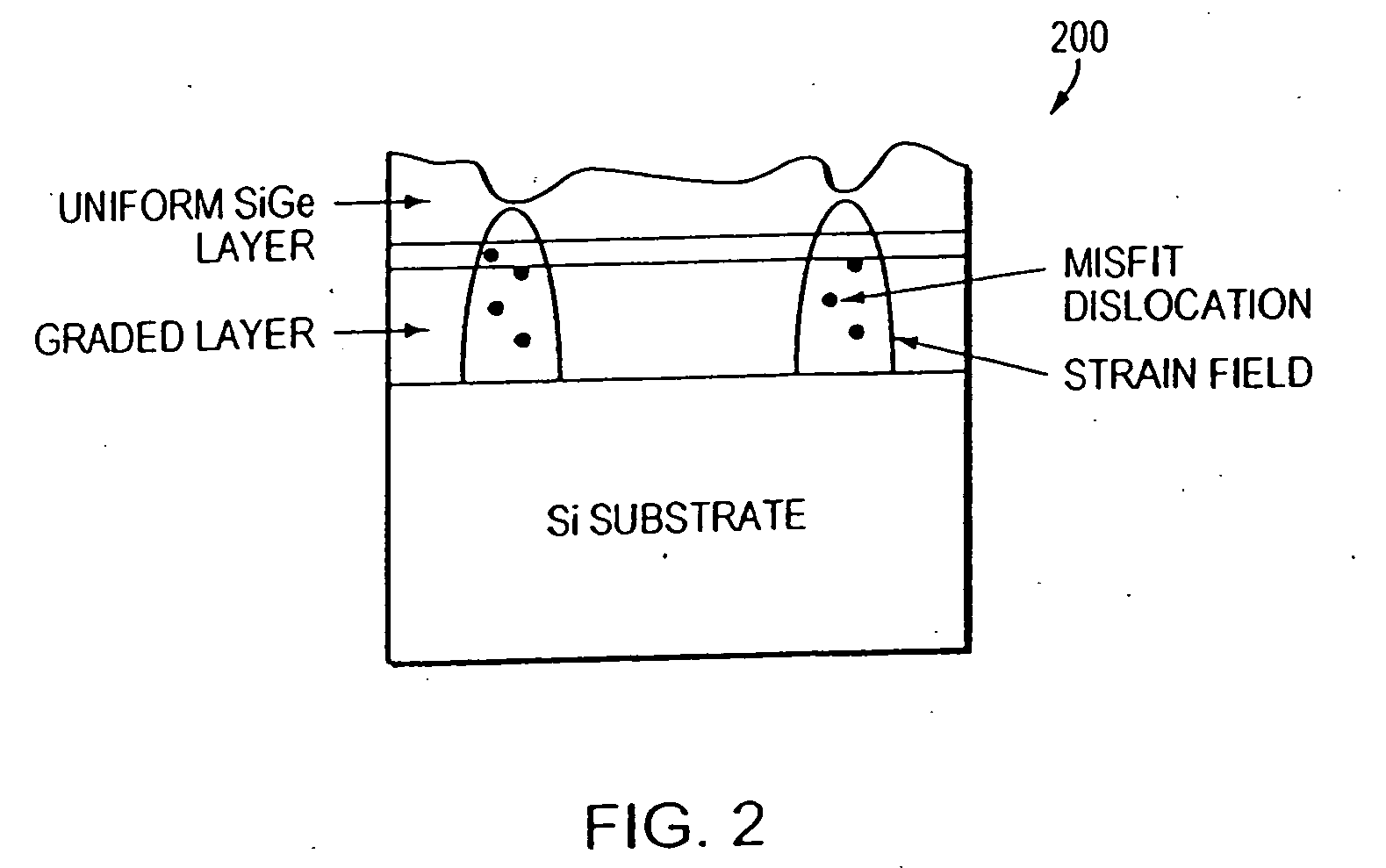
For more than 10 years, researchers have tried to intrinsically control the surface morphology through epitaxial growth, but since the stress fields from the misfit dislocations affect the growth front, no intrinsic epitaxial solution is possible.
A second problem with the strained Si devices made to date is that researchers have been concentrating on devices optimized for very different applications.

Method used


Image

  • Relaxed SiGe platform for high speed CMOS electronics and high speed analog circuits
  • Relaxed SiGe platform for high speed CMOS electronics and high speed analog circuits
  • Relaxed SiGe platform for high speed CMOS electronics and high speed analog circuits

Examples


Embodiment Construction

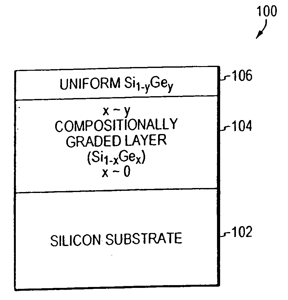
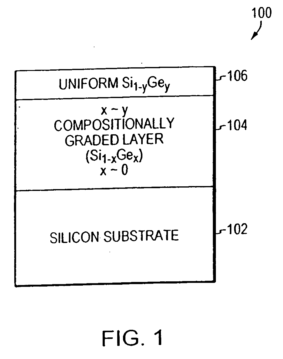
[0024]FIG. 1 is a schematic block diagram of a structure 100 including a relaxed SiGe layer epitaxially grown on a Si substrate 102. In this structure, a compositionally graded buffer layer 104 is used to accommodate the lattice mismatch between the uniform SiGe layer 106 and the Si substrate. By spreading the lattice mismatch over a distance, the graded buffer minimizes the number of dislocations reaching the surface and thus provides a method for growing high-quality relaxed SiGe films on Si.

[0025] Any method of growing a high-quality, relaxed SiGe layer on Si will produce roughness on the surface of the SiGe layer in a well-known crosshatch pattern. This crosshatch pattern is typically a few hundred angstroms thickness over distances of microns. Thus, the crosshatch pattern is a mild, undulating surface morphology with respect to the size of the electron or hole. For that reason, it is possible to create individual devices that achieve enhancements over their control Si device c...


PUM


Abstract

Structures and methods for fabricating high speed digital, analog, and combined digital / analog systems using planarized relaxed SiGe as the materials platform. The relaxed SiGe allows for a plethora of strained Si layers that possess enhanced electronic properties. By allowing the MOSFET channel to be either at the surface or buried, one can create high-speed digital and / or analog circuits. The planarization before the device epitaxial layers are deposited ensures a flat surface for state-of-the-art lithography.

Description

PRIORITY INFORMATION [0001] This application claims priority from provisional application Ser. No. 60 / 273,112 filed Mar. 2, 2001.BACKGROUND OF THE INVENTION [0002] The invention relates to the field of relaxed SiGe platforms for high speed CMOS electronics and high speed analog circuits. [0003] Si CMOS as a platform for digital integrated circuits has progressed predictably through the industry roadmap. The progress is created through device miniaturization, leading to higher performance, greater reliability, and lower cost. However, new bottlenecks in data flow are appearing as the interconnection hierarchy is expanded. Although digital integrated circuits have progressed at unprecedented rates, analog circuitry has hardly progressed at all. Furthermore, it appears that in the near future, serious economic and technological issues will confront the progress of digital integrated circuits. [0004] The digital and communication chip markets need an enhancement to Si CMOS and the matur...

Claims


Application Information

Patent Timeline
Patent Type & Authority Applications(United States)
IPC IPC(8): H01L21/20H01L21/337H01L21/762H01L21/8234H01L21/8238H01L27/092H01L29/10H01L29/78H01L29/80
CPCH01L21/02381H01L29/802H01L21/02505H01L21/0251H01L21/02532H01L21/76251H01L21/76256H01L21/823412H01L21/823807H01L27/092H01L29/1054H01L29/66893H01L29/66916H01L29/7838H01L21/0245
Inventor FITZERGALD, EUGENE A.
Owner TAIWAN SEMICON MFG CO LTD
Learn More