
Method of determining remaining film thickness in polishing process

Inactive Publication Date: 2005-04-14
LAPIS SEMICON CO LTD
View PDF3 Cites 4 Cited by
  • Summary
  • Abstract
  • Description
  • Claims
  • Application Information

AI Technical Summary

Benefits of technology

[0042] According to the second invention, since polish suppressing films are formed in a region in which the result of determination of the remaining film thickness in a polishing process is smaller than a predetermined film thickness, the remaining film thickness of a coated film can be highly accurately controlled by mere addition of a simple process.

Problems solved by technology

However, it was very difficult to control the polishing amount of CMP with high accuracy.
However, although the method for analyzing the section by the SEM is capable of accurately recognizing the remaining film thickness of the silicon nitride film 803, it causes a breakdown in the silicon substrate 801 and needs a large number of processes and much time for analysis.
However, when a region in which an active pattern density (proportion of area occupied by device forming regions) is extremely small, exists, it becomes difficult to control the accurate remaining film thickness of the silicon nitride film 803 in reverse.
This is because when the ceria slurry is used, the polishing speed becomes very fast.
However, the addition of such a design condition will increase the load on design.
Additionally, only the appropriateness of the design condition might encounter difficulties in controlling the polishing amount of CMP with high accuracy.
It is difficult to apply the present technique to a device isolating process.
However, the formation of the dummy trenches will incur degradation of the rate of integration of the semiconductor device and an increase in complexity, thus resulting in unreality.

Method used


Image

  • Method of determining remaining film thickness in polishing process
  • Method of determining remaining film thickness in polishing process
  • Method of determining remaining film thickness in polishing process

Examples


first embodiment

[0095] Incidentally, the present embodiment will explain as an example a case in which the method of the first embodiment is used as a method of determining the remaining film thickness in the polishing process.

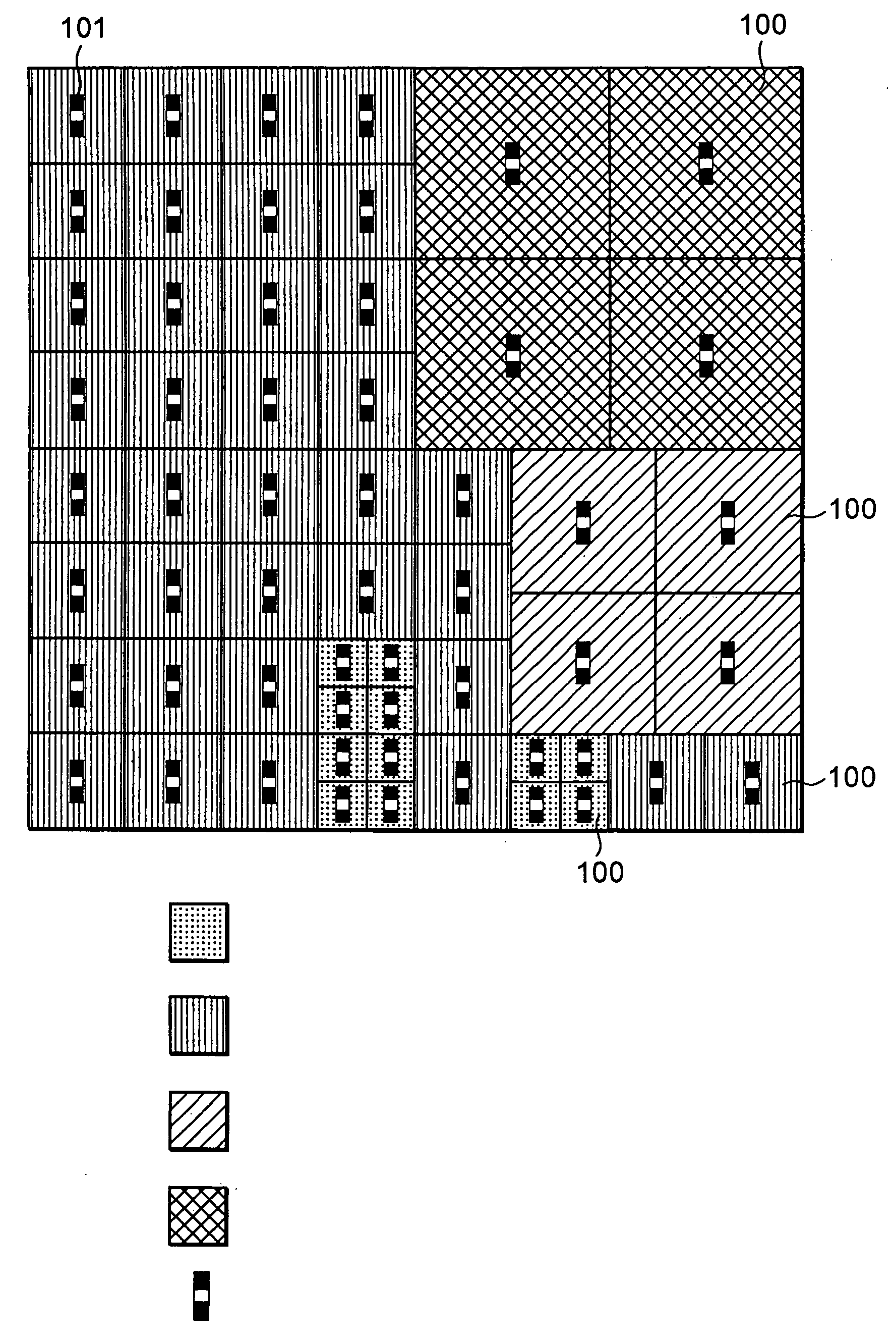
[0096]FIG. 7 is a plan view conceptually showing polish suppressing films (silicon nitride film patterns 701) according to the present embodiment.

[0097] In the example shown in FIG. 7, the size of each of the silicon nitride film patterns 701 is set to 2.5 μm×2.5 μm in a region in which a local active pattern density is less than 5%. The size thereof is set to 1 μm×1 μm in a region in which a local active pattern density ranges from over 5% to under 10%. The interval in which the silicon nitride film patterns 701 are laid out, is set to 0.5 μm regardless of the local active pattern density. Thus, the proportion of area occupied by the silicon nitride film patterns 701 results in 69.4% in the region in which the local active pattern density is less than 5% and results in 44.4...

second embodiment

[0098] According to the present embodiment as described above, since the proportion of area occupied by the polish suppressing films is changed according to the result of determination of the remaining film thickness in the polishing process, variations in the remaining film thickness of the silicon nitride film 503 can be further suppressed as compared with the

[0099] In a manner similar to the second embodiment, the reliability of suppression of variations in the remaining film thickness can be made very high where the determining method of the present invention is used as the method of determining the remaining film thickness in the polishing process. The present embodiment is similar to the second embodiment even in that other material films can be used as the polish suppressing films.

[0100] Although the proportion of area occupied by the polish suppressing films is divided into two stages in the present embodiment, it is needless to say that it may be divided into three stages....


PUM

PropertyMeasurementUnit
Thicknessaaaaaaaaaa

Abstract

The present invention of a method of determining remaining film thickness in polishing process can provide a technology for controlling a polishing amount of CMP in a device isolating process with satisfactory accuracy regardless of the ratio between the area of each of device forming regions and that of each of trench regions, the type of abrasive, etc.

Description

BACKGROUND OF THE INVENTION [0001] 1. Field of the Invention [0002] The present invention relates to a technology for performing device isolation of a semiconductor device by using a CMP (Chemical Mechanical Polishing) method. [0003] 2. Description of the Related Art [0004] As a device isolation technique used for a semiconductor device, there has been known, for example, an STI (Shallow Trench Isolation) technology. In the STI technology, device isolation is carried out by shallow trenches defined in the surface of a semiconductor substrate. [0005] One example of a device isolating process using the STI technology will be explained below with reference to FIGS. 8 and 9. [0006] (1) A protective oxide film 802 having a thickness of about 15 nm is formed on the surface of a silicon substrate 801. Subsequently, a silicon nitride (SiN) film 803 is formed on the surface of the protective oxide film 802 by, for example, an LPCVD (Low Pressure Chemical Vapor Deposition) method. Further, re...

Claims


Application Information

Patent Timeline
IPC IPC(8): H01L21/66H01L21/304H01L21/76
CPCH01L22/26
Inventor ASAKAWA, KAZUHIKO
Owner LAPIS SEMICON CO LTD
Features
  • Generate Ideas
  • Intellectual Property
  • Life Sciences
  • Materials
  • Tech Scout
  • Unparalleled Data Quality
  • Higher Quality Content
  • 60% Fewer Hallucinations
Learn More