Optical sensor device and electronic apparatus

a technology of optical sensors and electronic devices, applied in pulse generators, instruments, pulse techniques, etc., can solve the problems of large mounting space, high cost, and easy superimposed noise, and achieve the effect of reducing cost and mounting space, and reducing the noise of superimposed nois

Inactive Publication Date: 2005-04-21
SEMICON ENERGY LAB CO LTD
View PDF72 Cites 55 Cited by
  • Summary
  • Abstract
  • Description
  • Claims
  • Application Information

AI Technical Summary

Benefits of technology

[0041] As described hereinbefore, in an optical sensor device according to the invention, a photodiode and an amplifier circuit using a TFT ...

Problems solved by technology

The above-described conventional optical sensor device is configured by the combination of the amorphous silicon photodiode 502, the external amplifier circuit 501, and the feedback resistor 503, causing problems s...

Method used


Image

  • Optical sensor device and electronic apparatus
  • Optical sensor device and electronic apparatus
  • Optical sensor device and electronic apparatus

Examples


embodiment mode 1

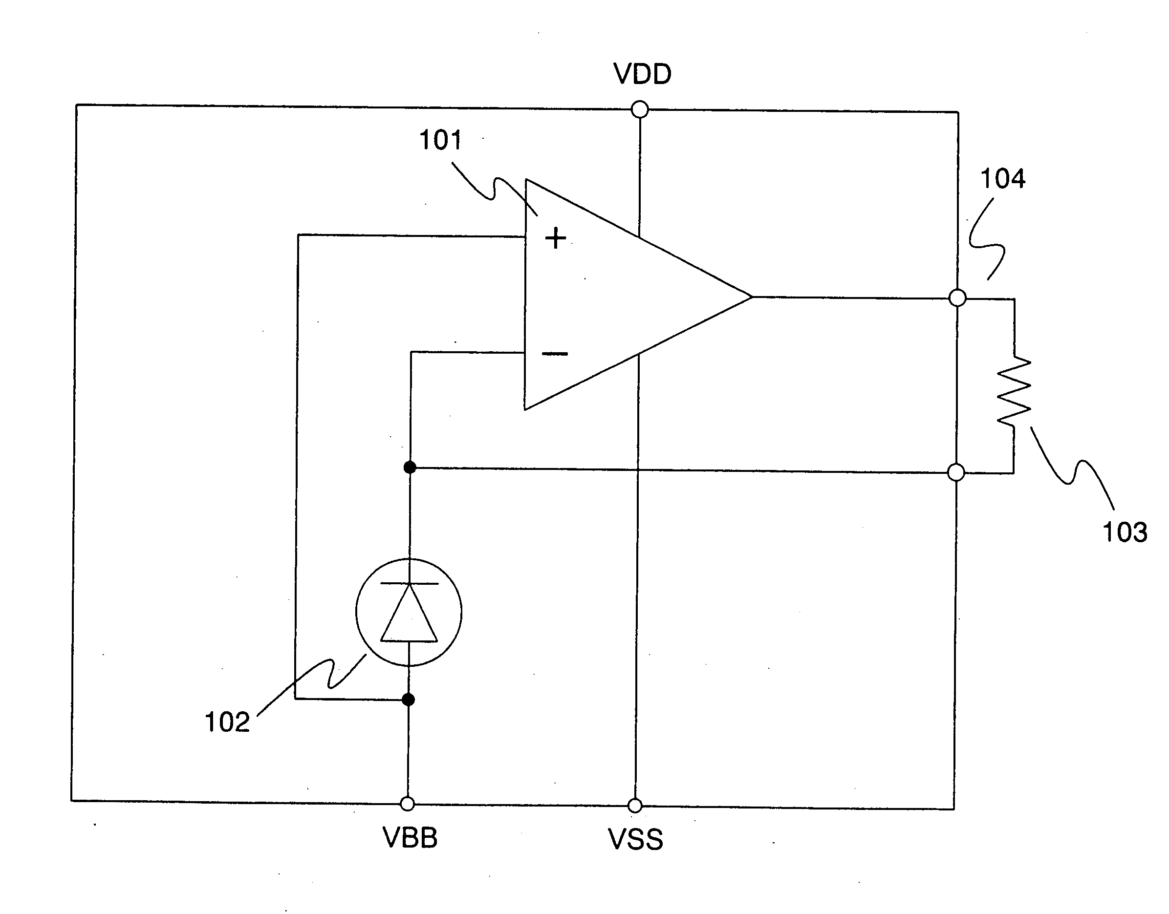
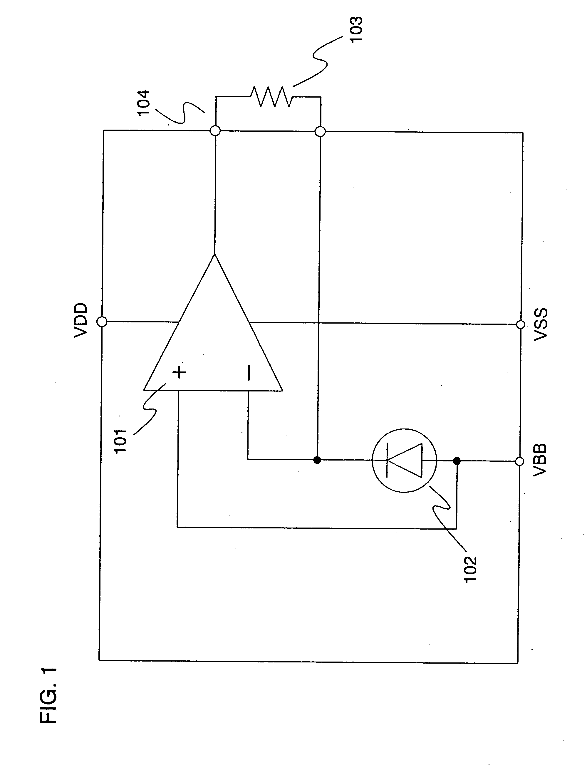
[0072]FIG. 1 shows the first embodiment mode of the invention. In this embodiment mode, an amplifier circuit 101 configured by a TFT and a photodiode 102 are formed integrally over a sensor substrate. An operation thereof is described below. A non-inverting input terminal of the amplifier circuit 101 is connected to an external power source VBB. The external power source VBB has a potential between a high-potential-side power source VDD and a low-potential-side power source VSS of the amplifier circuit 101. A first electrode of the photodiode 102 is connected to the external power source VBB and a second electrode thereof is connected to an inverting input terminal of the amplifier circuit 101 and a first terminal of a feedback resistor 103. A second terminal of the feedback resistor 103 is connected to an output terminal 104 of the amplifier circuit 101. Note that the feedback resistor 103 is formed outside of the sensor substrate in order to reduce the fluctuation of an output vol...

embodiment mode 2

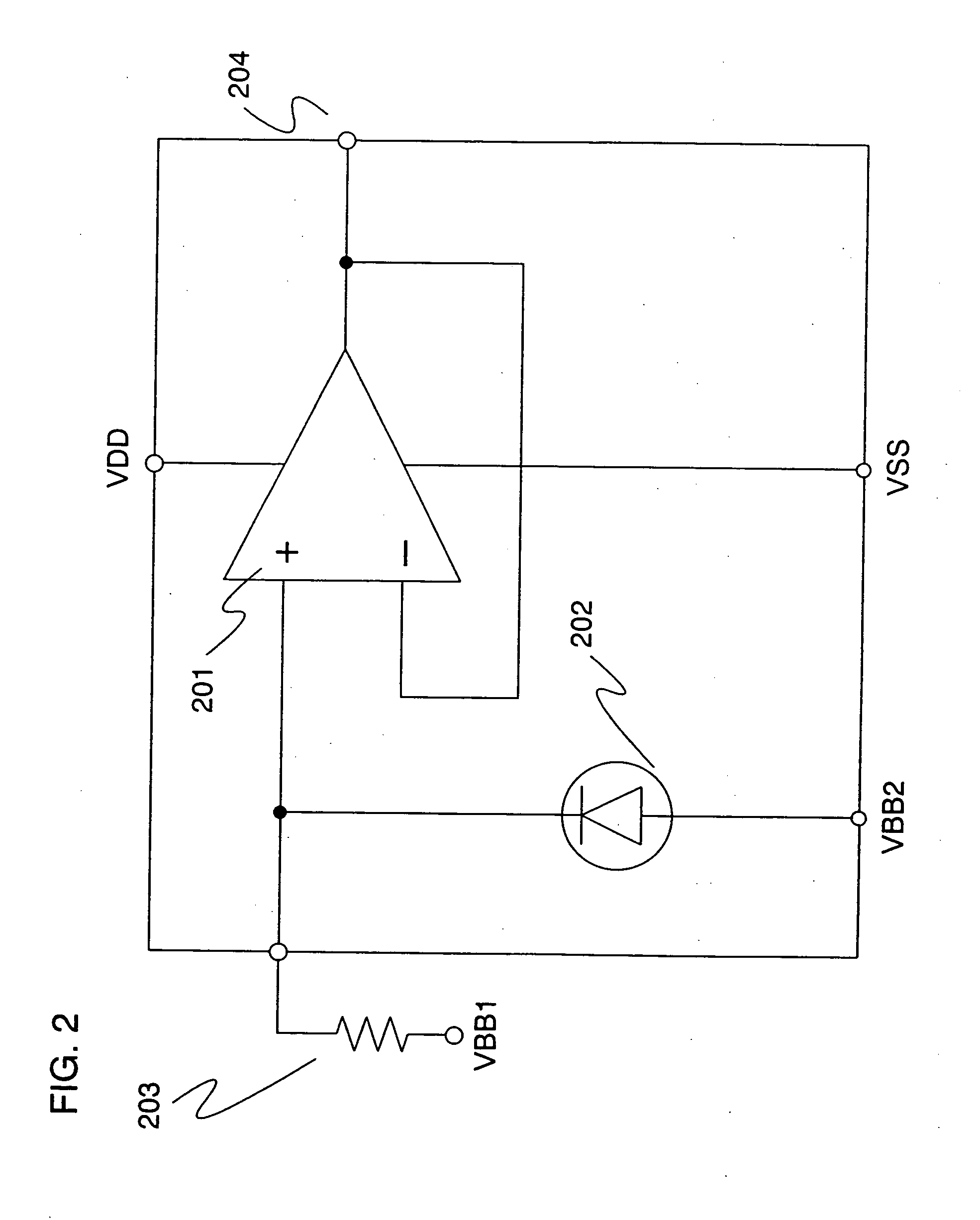
[0078]FIG. 2 shows the second embodiment mode of the invention. In this embodiment mode, an amplifier circuit 201 configured by a TFT and a photodiode 202 are formed integrally over a sensor substrate. An operation thereof is described below. A non-inverting input terminal of the amplifier circuit 201 is connected to a first terminal of an I-V conversion resistor 203 and a second electrode of the photodiode 202. An output terminal 204 of the amplifier circuit 201 is connected to an inverting terminal thereof, that is, the amplifier circuit 201 is a voltage follower. A first electrode of the photodiode 202 is connected to an external power source VBB2. A second terminal of the I-V conversion resistor 203 is connected to an external power source VBB1. Note that the I-V conversion resistor 203 is formed outside of the sensor substrate in order to reduce the fluctuation of an output voltage, however, the I-V conversion resistor 203 may be formed over the sensor substrate in the case whe...

embodiment mode 3

[0085]FIG. 3 shows the third embodiment mode of the invention. In this embodiment mode, an amplifier circuit 301 configured by a TFT, a photodiode 302, and level shift circuits 305 and 306 are formed integrally over a sensor substrate. An operation thereof is described below. An input of the level shift circuit 305 is connected to a low-potential-side power source VSS and an output thereof is connected to a non-inverting input terminal of the amplifier circuit 301. An input of the level shift circuit 306 is connected to a second electrode of the photodiode 302 and a first terminal of a feedback resistor 303 and an output thereof is connected to an inverting input terminal of the amplifier circuit 301. A second terminal of the feedback resistor 303 is connected to an output terminal 304 of the amplifier circuit 301. A first electrode of the photodiode 302 is connected to the low-potential-side power source VSS. Note that the feedback resistor 303 is formed outside of the sensor subst...


PUM


Abstract

In an optical sensor device employing an amorphous silicon photodiode, an external amplifier IC and the like are required due to low current capacity of the sensor element in order to improve the load driving capacity. It leads to increase in cost and mounting space of the optical sensor device. In addition, noise may easily superimpose since the photodiode and the amplifier IC are connected to each other over a printed circuit board. According to the invention, an amorphous silicon photodiode and an amplifier configured by a thin film transistor are formed integrally over a substrate so that the load driving capacity is improved while reducing cost and mounting space. Superimposing noise can be also reduced.

Description

BACKGROUND OF THE INVENTION [0001] 1. Field of the Invention [0002] The present invention relates to an optical sensor device, and particularly to an optical sensor device configured by a thin film semiconductor element. Further, the invention relates to an electronic apparatus using the optical sensor device. [0003] 2. Description of the Related Art [0004] In recent years, cellular phones have been widely used with the advance of telecommunication technology. In future, transmission of moving images and transmission of a larger volume of information are expected. In addition, through reduction in weight of personal computers, those adapted for mobile communication have been produced. Information terminals called PDAs originated in electronic notebooks have also been produced in large quantities and widely used. With the development of display devices, the majority of portable information devices is equipped with a flat panel display. [0005] In such a display device, brightness of t...

Claims


Application Information

Patent Timeline
IPC IPC(8): H01J40/14
CPCH01L27/12H01L27/14692H01L27/14609
Inventor KOYAMA, JUNOSADA, TAKESHIMATSUZAKI, TAKANORINISHI, KAZUOMARUYAMA, JUNYA
Owner SEMICON ENERGY LAB CO LTD
Why Eureka
Try Eureka