Electroluminescence display device

a display device and electroluminescent technology, applied in the direction of static indicating devices, identification means, instruments, etc., can solve the problem that the leak current generated in the other conductive region connected to the el element cannot be controlled, and achieve the effect of reducing the generation of leak current, sharp display, and improving color reproducibility of gray colors

Inactive Publication Date: 2005-04-21
SANYO ELECTRIC CO LTD
View PDF10 Cites 34 Cited by
  • Summary
  • Abstract
  • Description
  • Claims
  • Application Information

AI Technical Summary

Benefits of technology

[0036] Consequently, in contrast to related art devices wherein image areas to be displayed in gray are displayed whiter than proper and color reproducibility in each of gray levels is lost, the present invention suppresses generation of a leak current, thereby improving color reproducibility of gray colors. Further, as a light shielding film having an opening corresponding to a portion (emissive layer) of the EL element is employed, a sharp display is obtained for each pixel and improvement in image sharpness and mixture in color can be achieved.

Problems solved by technology

While the leak current generated in the interface of one of the first and second or the third and fourth conductive regions of the TFT is controlled by a gate electrode before flowing into the EL element, the leak current generated in the other conductive region connected to the EL element cannot be controlled and flows into the EL element.

Method used


Image

  • Electroluminescence display device
  • Electroluminescence display device
  • Electroluminescence display device

Examples


Embodiment Construction

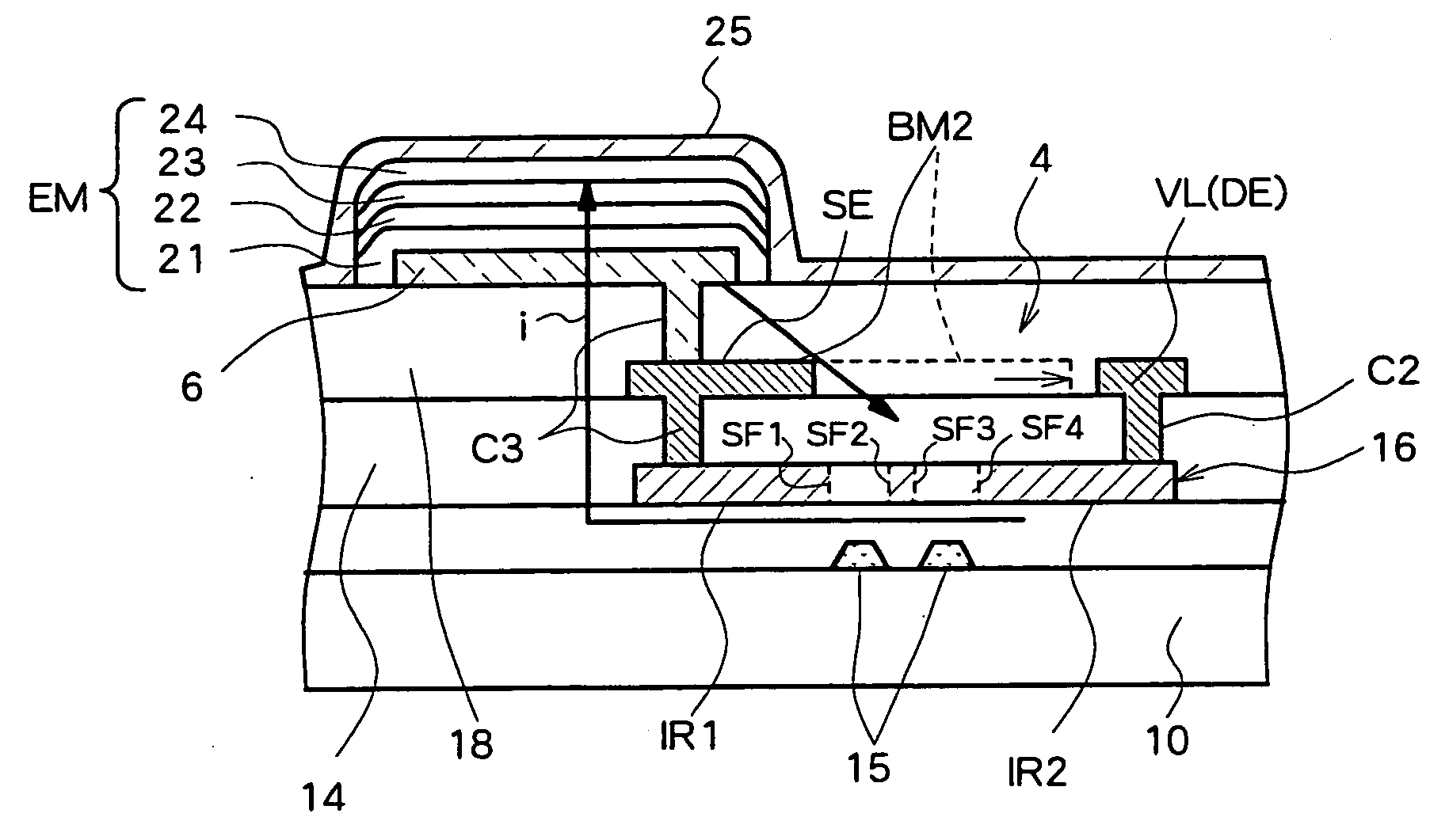
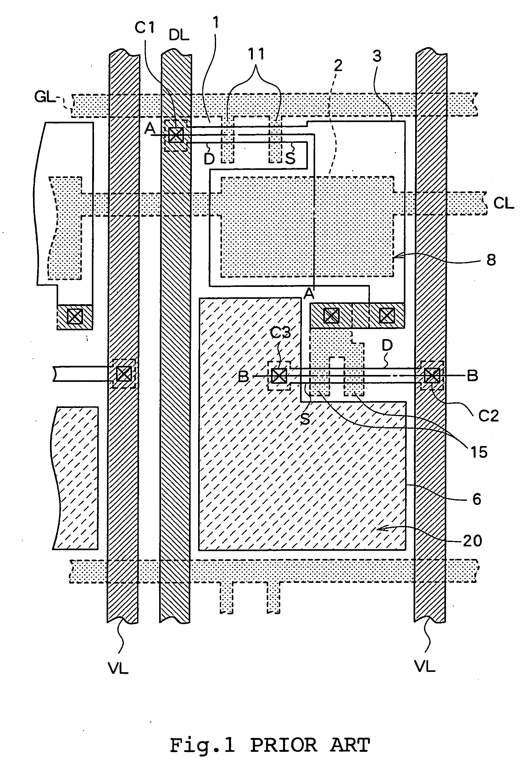
[0047] Preferred embodiments of the electroluminescence display device of the present invention will now be described. FIG. 3 is a plan view illustrating a display pixel of an EL display device of a bottom gate type. Regions surrounded by dotted lines and shaded by dots are a gate line GL, gate electrodes 11 and 15, a first capacitor electrode 2, and a line CL, formed of a gate material. Regions surrounded by solid lines and without hatching are formed of a Si layer (P—Si layer in this example), namely, active layers 12 and 16 of the TFTs and a second capacitor electrode 3 formed integrally with the active layer 12. A region provided in a lower part of the pixel and surrounded by solid lines in the figure is a transparent electrode serving as an anode 6 of the EL element. Regions surrounded by solid lines and indicated by hatching with slant lines are lines VL, DL and 30, and a light shielding layer BM, containing Al as a main material.

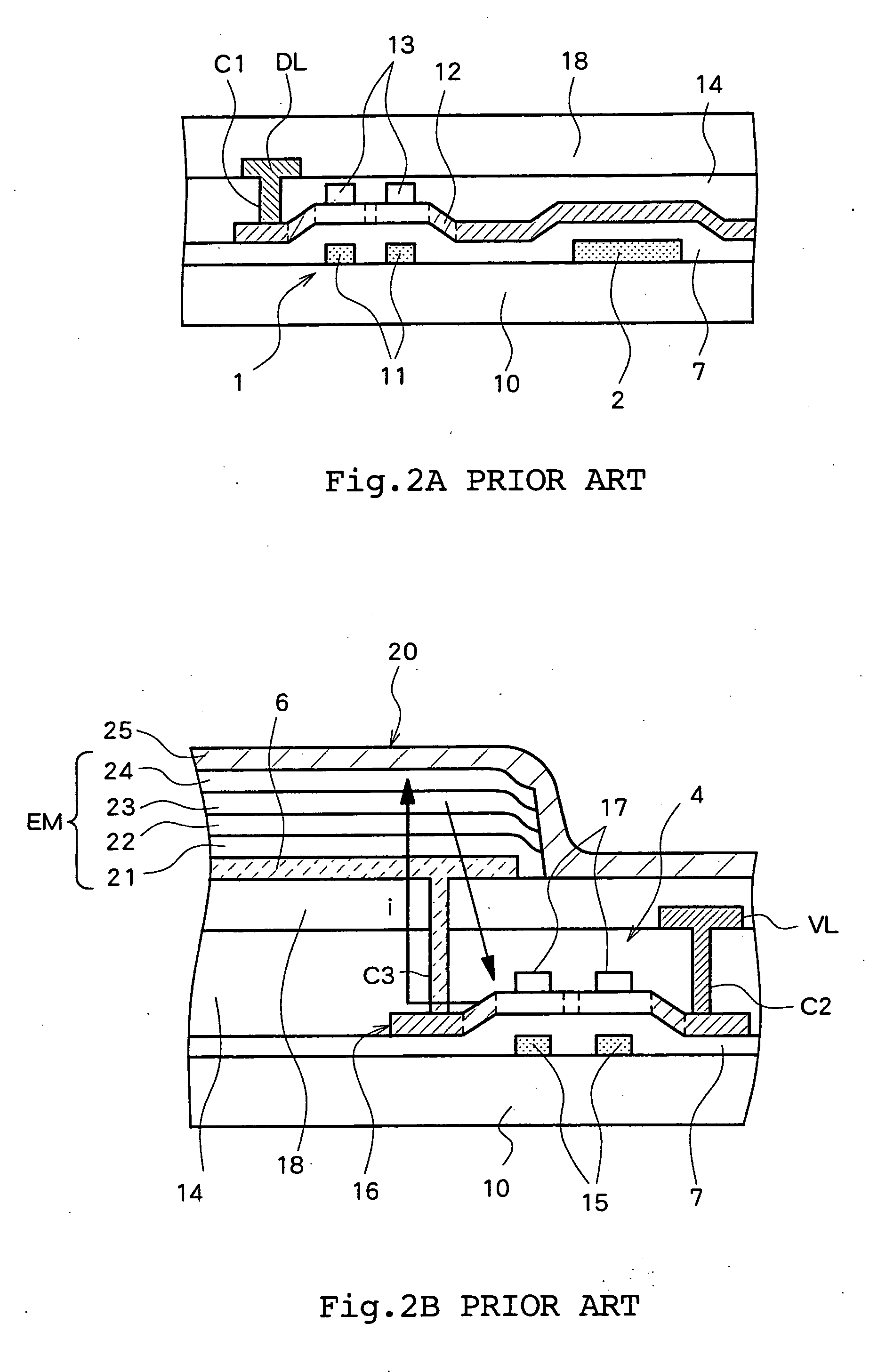
[0048]FIG. 4 and FIG. 5 are enlarged views cor...


PUM


Abstract

An EL element and an interface between a channel and an impurity diffusion area of a thin film transistor provided in the vicinity of the EL element are spaced apart. A light shielding film is provided between the EL element and the interface. By providing such a space and/or the light shielding film, generation of a leak current, which would otherwise be caused by light emitted from the self-emissive EL element entering the TFT, is reliably prevented, thereby ensuring that emitted light is not brighter than a predetermined luminance.

Description

BACKGROUND OF THE INVENTION [0001] 1. Field of the Invention [0002] The present invention relates to an electroluminescence display device comprising electroluminescence elements and thin film transistors. [0003] 2. Description of the Prior Art [0004] In recent years, electroluminescence (referred to herein after as “EL”) display devices comprising EL elements have gained attention as potential replacements for CRTs and LCDs. Research has been directed to the development of EL display devices using, for example, thin film transistors (referred to hereinafter as “TFT”) as switching elements to drive the EL elements. [0005]FIG. 1 is a plan view showing a display pixel of an organic EL display device. FIG. 2A shows a cross-sectional view taken along line A-A of FIG. 1 while FIG. 2B shows a cross-sectional view taken along line B-B of FIG. 1. [0006] As shown in these drawings, a display pixel 20 is formed in a region surrounded by a gate line GL and a data line DL. A first TFT serving a...

Claims


Application Information

Patent Timeline
Patent Type & Authority Applications(United States)
IPC IPC(8): G09G3/30G09F9/30H01L21/336H01L27/32H01L29/04H01L29/786H01L51/50H01L51/52H05B33/00H05B33/02H05B33/12H05B33/14H05B33/22
CPCH01L27/3262H01L51/5284H01L27/3272H10K59/126H10K59/1213H10K50/865H05B33/00
Inventor NISHIKAWA, RYUJI
Owner SANYO ELECTRIC CO LTD
Why Eureka
Try Eureka