Germanate gate dielectrics for semiconductor devices

a germanate and gate dielectric technology, applied in the field of germanate gate dielectrics, can solve the problems of gate dielectrics, high device mobility, and complex technology, and achieve the effect of high ion polarization and high dielectric constan

Inactive Publication Date: 2005-04-21
IBM CORP
View PDF9 Cites 36 Cited by
  • Summary
  • Abstract
  • Description
  • Claims
  • Application Information

AI Technical Summary

Benefits of technology

[0008] It is a further object of the present invention to teach processors which comprise chips containing such a semiconductor field effect device having a germanate gate dielectric.

Problems solved by technology

As MOSFET (Metal Oxide Semiconductor Field-Effect-Transistor, a name with historic connotations meaning in general an insulated gate Field-Effect-Transistor) devices are being scaled down, the technology becomes more complex and new methods are needed to maintain the expected performance enhancement from one generation of devices to the next.
There is great difficulty in keeping carrier mobility high in devices of deeply submicron generations.
Gate dielectrics is one of the main problems for CMOS field effect device scaling.
In Ge-based devices, the situation is even more complicated.
Up to now, no reliable high-quality gate dielectric has been found.
Germanium oxide is of poor quality and is soluble in water.
Another issue with binary oxides is interface instability, i.e. a thin lower-K material (e.g. SiO2, SiON, or GeON) is present at the interface which is either deliberately grown there before high-K deposition, or formed due to reactions at high temperatures.

Method used


Image

  • Germanate gate dielectrics for semiconductor devices
  • Germanate gate dielectrics for semiconductor devices
  • Germanate gate dielectrics for semiconductor devices

Examples


Embodiment Construction

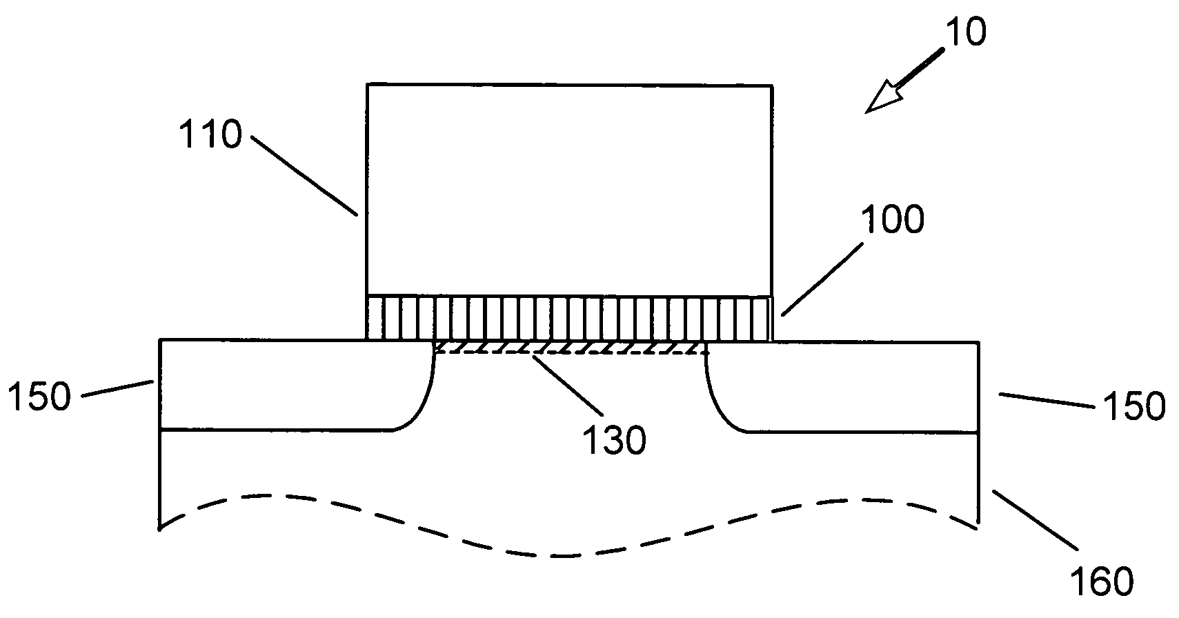
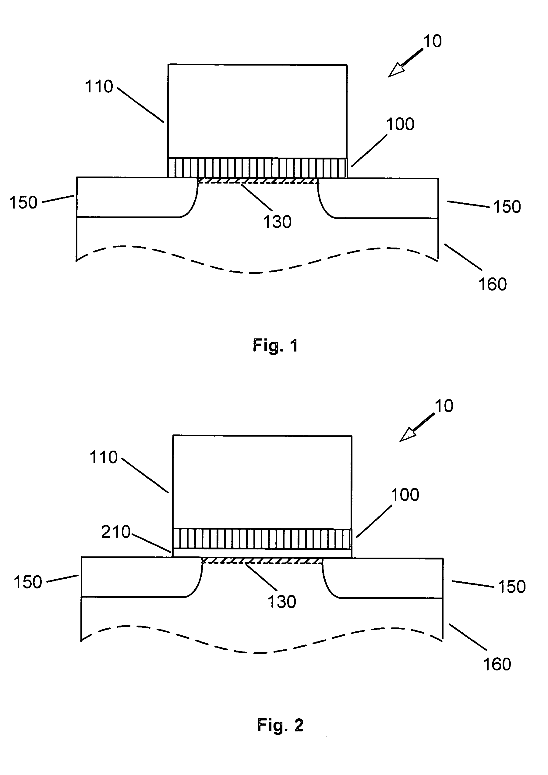
[0013]FIG. 1 shows a schematic cross sectional view of a semiconductor field effect device 10 having a germanate gate dielectric. The gate dielectric of a germanate material 100 is an insulator separating a conductive gate 110 from a semiconductor body 160.

[0014] Germanate materials have a chemical composition of MezGexOy, where x, y, and z are non-zero integers, in a very wide variety of possible combinations. The “Me” stands for a metal with high ion polarizability, resulting in a high dielectric constant for the germanate material. A non-exhaustive list of such metals include: Hf, Zr, Y, La, Ti, Ta, Gd, Ce, Bi, Dy, Er, Eu, Tb, Pr, Sr, etc., as well as some further metals of group 3, 4 and 5 of the periodic table and lanthanides. Metal polarizabilities are known in the art, for instance polarizabilities of various elements is given in the publication: “Dielectric Polarizabilities of ions in oxides and fluorides”, J. of Applied Physics, v. 73, p. 348 (1993). Germanate materials ar...


PUM

PropertyMeasurementUnit
dielectric constantaaaaaaaaaa

Abstract

A structure, and method of fabrication, for high performance semiconductor field effect devices is disclosed. These devices are having a gate dielectric containing a germanate material. In representative embodiments the gate dielectric is essentially a layer of a germanate material. The chemical composition of such materials is MezGexOy, where Me stands for a metal with high ion polarizability, and x, y, and z are non-zero integers. Such a gate dielectric is advantageous, from the point of view of dielectric constant, barrier height, carrier mobility, thermal stability, and interface stability.

Description

FIELD OF THE INVENTION [0001] The present invention relates to a new class of gate dielectric materials allowing better device properties and expanded device choice in the deeply submicron, high performance regime. More specifically, the invention teaches gate dielectrics formed with germanate materials. BACKGROUND OF THE INVENTION [0002] Today's integrated circuits include a vast number of devices. Smaller devices are key to enhance performance and to improve reliability. As MOSFET (Metal Oxide Semiconductor Field-Effect-Transistor, a name with historic connotations meaning in general an insulated gate Field-Effect-Transistor) devices are being scaled down, the technology becomes more complex and new methods are needed to maintain the expected performance enhancement from one generation of devices to the next. [0003] One of the most important indicators of potential device performance is the carrier mobility. There is great difficulty in keeping carrier mobility high in devices of ...

Claims


Application Information

Patent Timeline
Patent Type & Authority Applications(United States)
IPC IPC(8): H01L21/28H01L21/316H01L29/51
CPCH01L21/28194H01L21/28264H01L29/518H01L29/517H01L21/31604H01L21/02271H01L21/0228H01L21/02112
Inventor GOUSEV, EVGENICALLEGARI, ALESSANDRO CESARELACEY, DIANNE L.NEUMAYER, DEBORAH ANNSHANG, HUILING
Owner IBM CORP
Why Eureka
Try Eureka