

Solid-state imaging device and method of manufacturing the same
a solid-state imaging and imaging device technology, applied in the direction of color television, television system, radio control device, etc., can solve the problems of reverse-direction leakage current at a pn, degrade the performance of the solid-state imaging device, and state imaging device, so as to suppress image defects sufficiently and improve the readout characteristic
- Summary
- Abstract
- Description
- Claims
- Application Information
AI Technical Summary
Benefits of technology
Problems solved by technology
Method used
Image

Examples
first embodiment
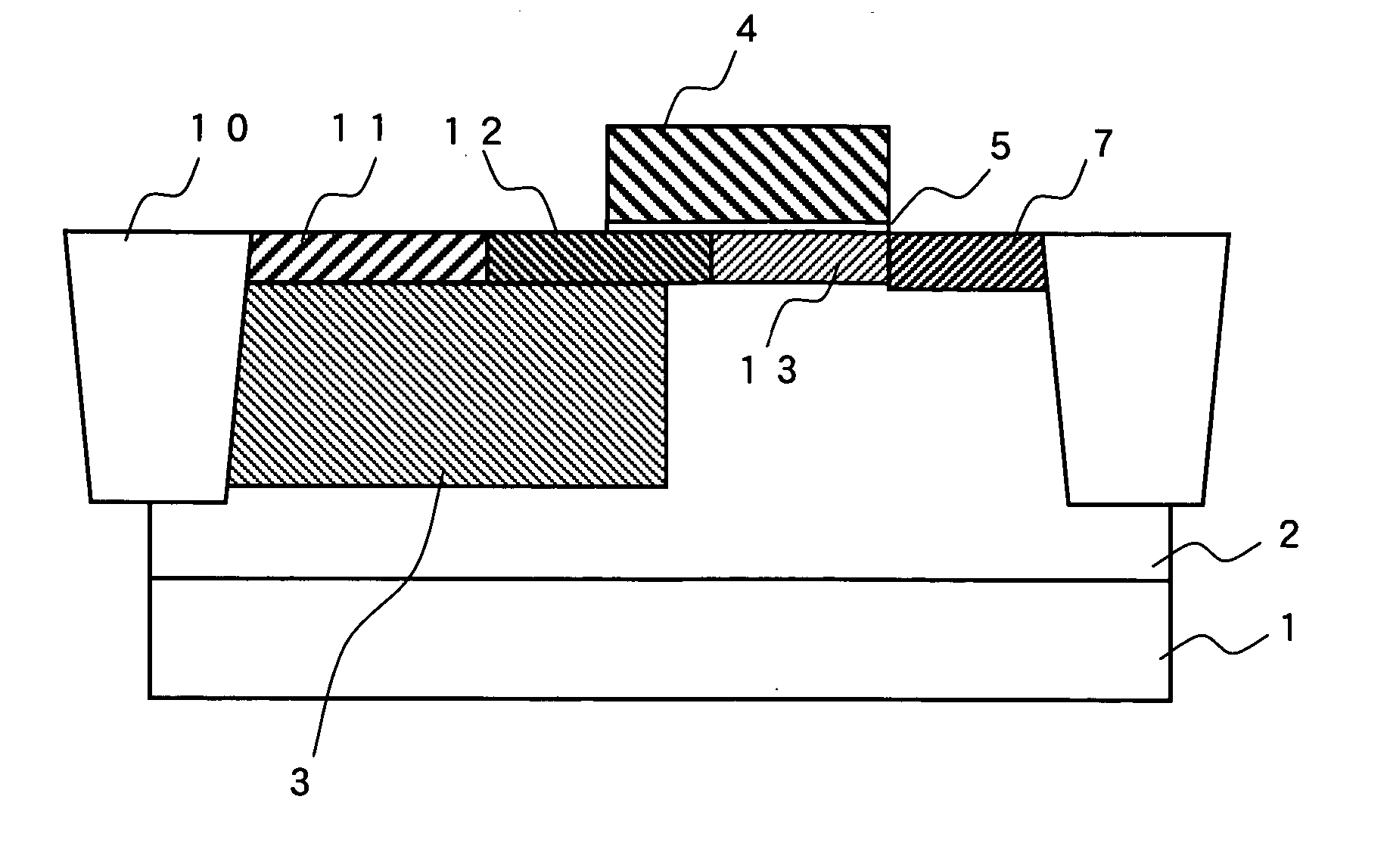
[0022]FIG. 1 is a cross-sectional view showing a cell structure of a solid-state imaging device according to a first embodiment. Inside a P-well 2 of a Si substrate 1, a N-type photodiode region 3 for photoelectrically converting incident light is formed. A gate electrode 4 is disposed so that one edge thereof forms an overlapping region with the photodiode region 3. Adjacent to the other edge of the gate electrode 4, an N-type drain region 7 is formed. Under the gate electrode 4, a gate oxide film 5 having a thickness of not more than 10 nm is formed. An element-isolating portion 10 having a STI (Shallow Trench Isolation) structure isolates respective elements composed of a photodiode and a plurality of MOS transistors.
[0023] On the surface portion of the photodiode region 3, a P-type first region 11 having a P-type first concentration and a P-type second region 12 having a P-type second concentration are formed. In a region adjacent to the P-type second region 12 and extending to...
second embodiment
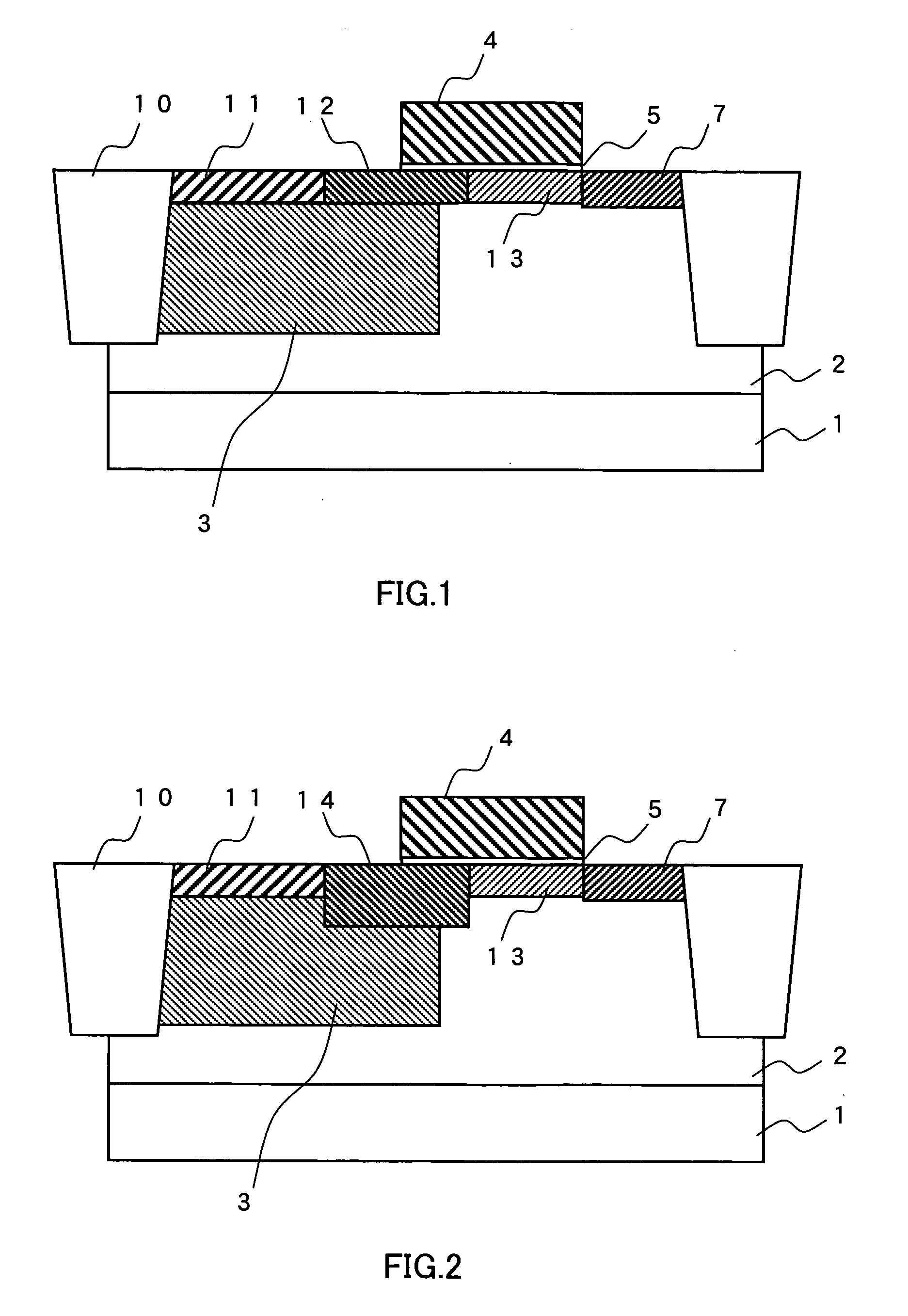
[0027]FIG. 2 is a cross-sectional view showing a cell structure of a solid-state imaging device of a second embodiment. Identical reference numbers are used for components common to those of the first embodiment described above, and detailed explanation will be omitted for these components.
[0028] In this embodiment, a P-type second-A region 14 is formed in place of the P-type second region 12 of the first embodiment. The P-type second-A region 14 is characterized in that a bottom of the P-type diffusion layer is positioned deeper than bottoms of the P-type diffusion layers of the P-type first region 11 and the P-type third region 13. For positioning the bottom of the P-type diffusion layer of the P-type second-A region 14 deeper than those of the P-type first region and the P-type third region, the acceleration energy of ion implantation is increased. That is, when E1 denotes an acceleration energy of the P-type first region 11, E2A denotes an acceleration energy of the P-type seco...
third embodiment
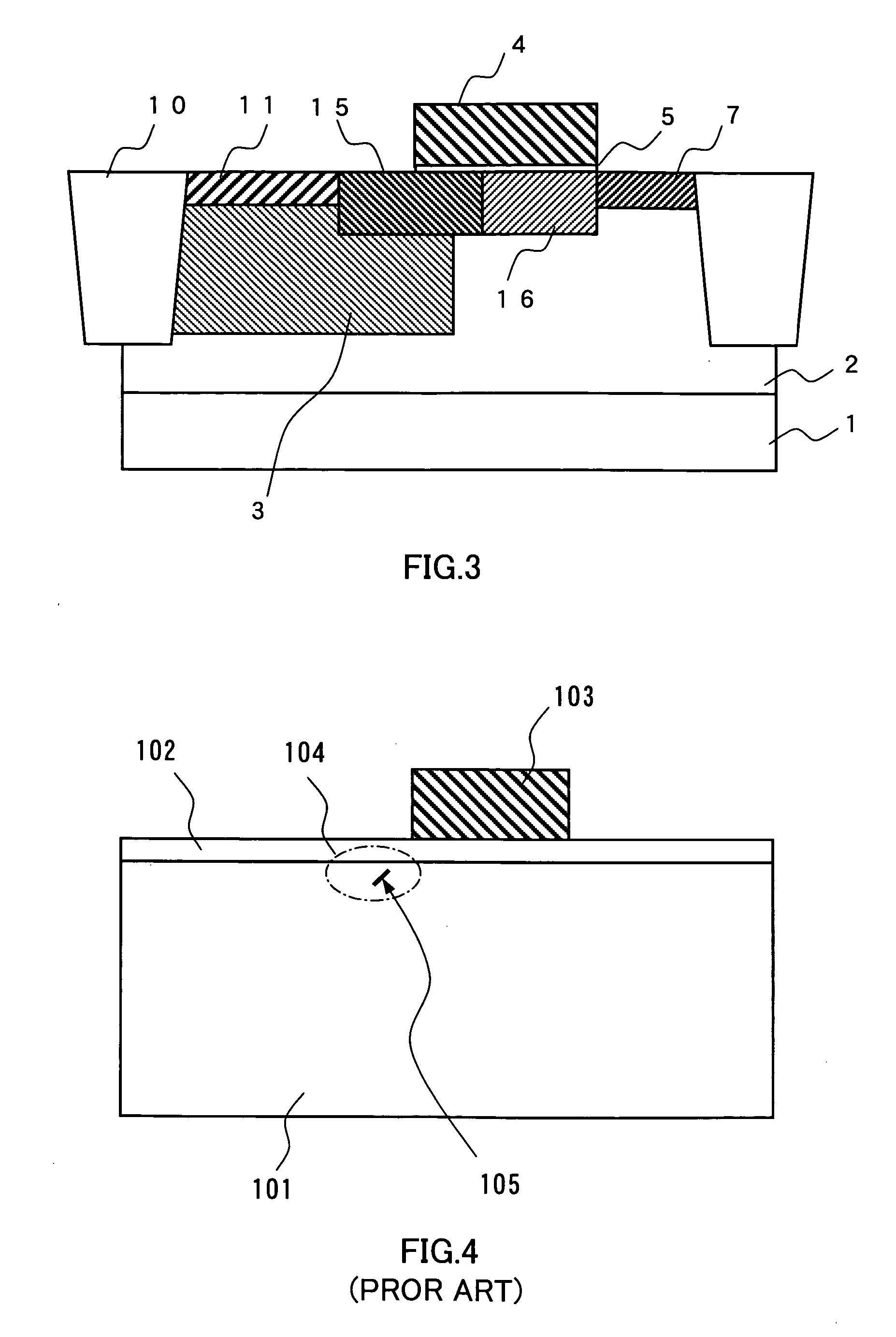
[0030]FIG. 3 is a cross-sectional view showing a cell structure of a solid-state imaging device according to a third embodiment. Identical reference numbers are used for components common to those of the first embodiment described above, and detailed explanation will be omitted for these components.
[0031] In this embodiment, a P-type second-B region 15 and a P-type third-A region 16 are formed in place of the P-type second region 12 and the P-type third region 13 of the first embodiment. This embodiment is characterized in that bottoms of the P-type diffusion layers of the P-type second-B region 15 and of the P-type third-A region 16 are positioned deeper than the bottoms of the P-type first region 11. For obtaining this structure, the energy of ion implantation during formation of the P-type difffusion layers is increased so as to position the bottoms of the P-type difffusion layers of the P-type second-B region 15 and of the P-type third A region 16 deeper than the bottom of the ...
PUM
 Abstract
Description
Claims
Application Information