Solid-state imaging device and method of manufacturing the same

a solid-state imaging and imaging device technology, applied in the direction of color television, television system, radio control device, etc., can solve the problems of reverse-direction leakage current at a pn, degrade the performance of the solid-state imaging device, and state imaging device, so as to suppress image defects sufficiently and improve the readout characteristic

Inactive Publication Date: 2006-04-18
COLLABO INNOVATIONS INC
View PDF11 Cites 7 Cited by
  • Summary
  • Abstract
  • Description
  • Claims
  • Application Information

AI Technical Summary

Benefits of technology

[0007]Therefore, with the foregoing in mind, it is an object of the present invention to provide a solid-state imaging device that has an improved readout characteristic at a low voltage and that suppresses image defects sufficiently.

Problems solved by technology

A most serious problem for the solid-state imaging device is a reverse-direction leakage current at a pn junction of a silicon semiconductor.
This leakage current, which cannot be isolated from a signal current generated by incident light, becomes a noise and degrades the performance of the solid-state imaging device.
However, when the concentration of the P-type diffusion layer 8 in the vicinity of the gate electrode 4 is reduced, the interface state of the Si—SiO2 interface and the active level in the Si substrate 1 cannot be inactivated sufficiently, which may cause problems such as image defects (e.g., white flaws and dark current).

Method used


Image

  • Solid-state imaging device and method of manufacturing the same
  • Solid-state imaging device and method of manufacturing the same
  • Solid-state imaging device and method of manufacturing the same

Examples


first embodiment

(First Embodiment)

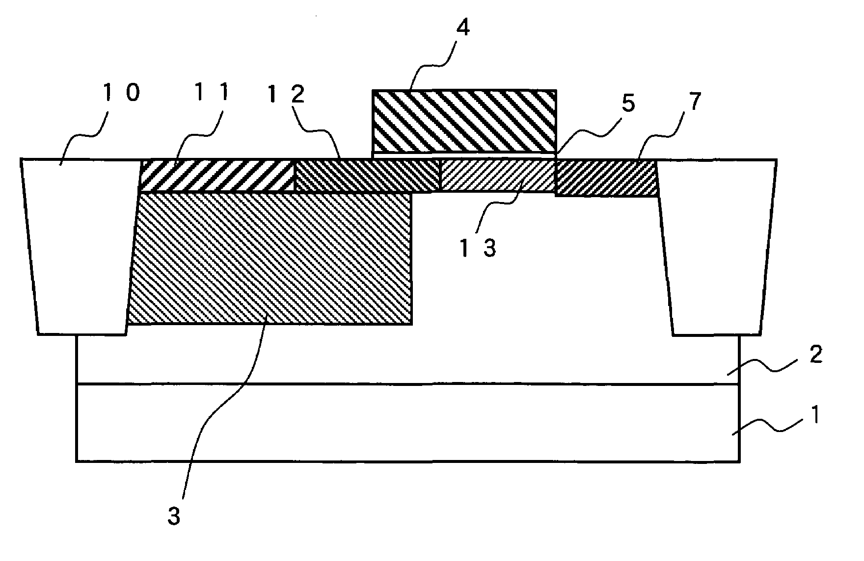
[0022]FIG. 1 is a cross-sectional view showing a cell structure of a solid-state imaging device according to a first embodiment. Inside a P-well 2 of a Si substrate 1, a N-type photodiode region 3 for photoelectrically converting incident light is formed. A gate electrode 4 is disposed so that one edge thereof forms an overlapping region with the photodiode region 3. Adjacent to the other edge of the gate electrode 4, an N-type drain region 7 is formed. Under the gate electrode 4, a gate oxide film 5 having a thickness of not more than 10 nm is formed. An element-isolating portion 10 having a STI (Shallow Trench Isolation) structure isolates respective elements composed of a photodiode and a plurality of MOS transistors.

[0023]On the surface portion of the photodiode region 3, a P-type first region 11 having a P-type first concentration and a P-type second region 12 having a P-type second concentration are formed. In a region adjacent to the P-type second region 12 ...

second embodiment

(Second Embodiment)

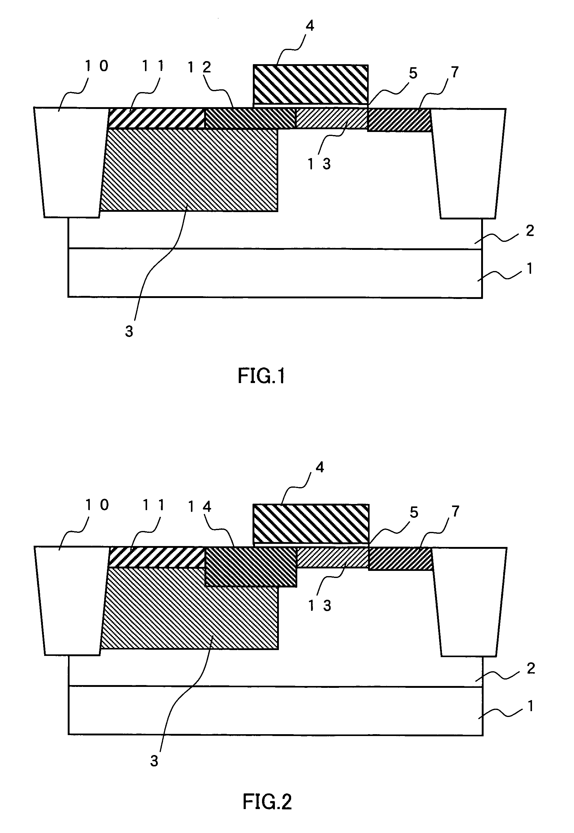
[0027]FIG. 2 is a cross-sectional view showing a cell structure of a solid-state imaging device of a second embodiment. Identical reference numbers are used for components common to those of the first embodiment described above, and detailed explanation will be omitted for these components.

[0028]In this embodiment, a P-type second-A region 14 is formed in place of the P-type second region 12 of the first embodiment. The P-type second-A region 14 is characterized in that a bottom of the P-type diffusion layer is positioned deeper than bottoms of the P-type diffusion layers of the P-type first region 11 and the P-type third region 13. For positioning the bottom of the P-type diffusion layer of the P-type second-A region 14 deeper than those of the P-type first region and the P-type third region, the acceleration energy of ion implantation is increased. That is, when E1 denotes an acceleration energy of the P-type first region 11, E2A denotes an acceleration energy o...

third embodiment

(Third Embodiment)

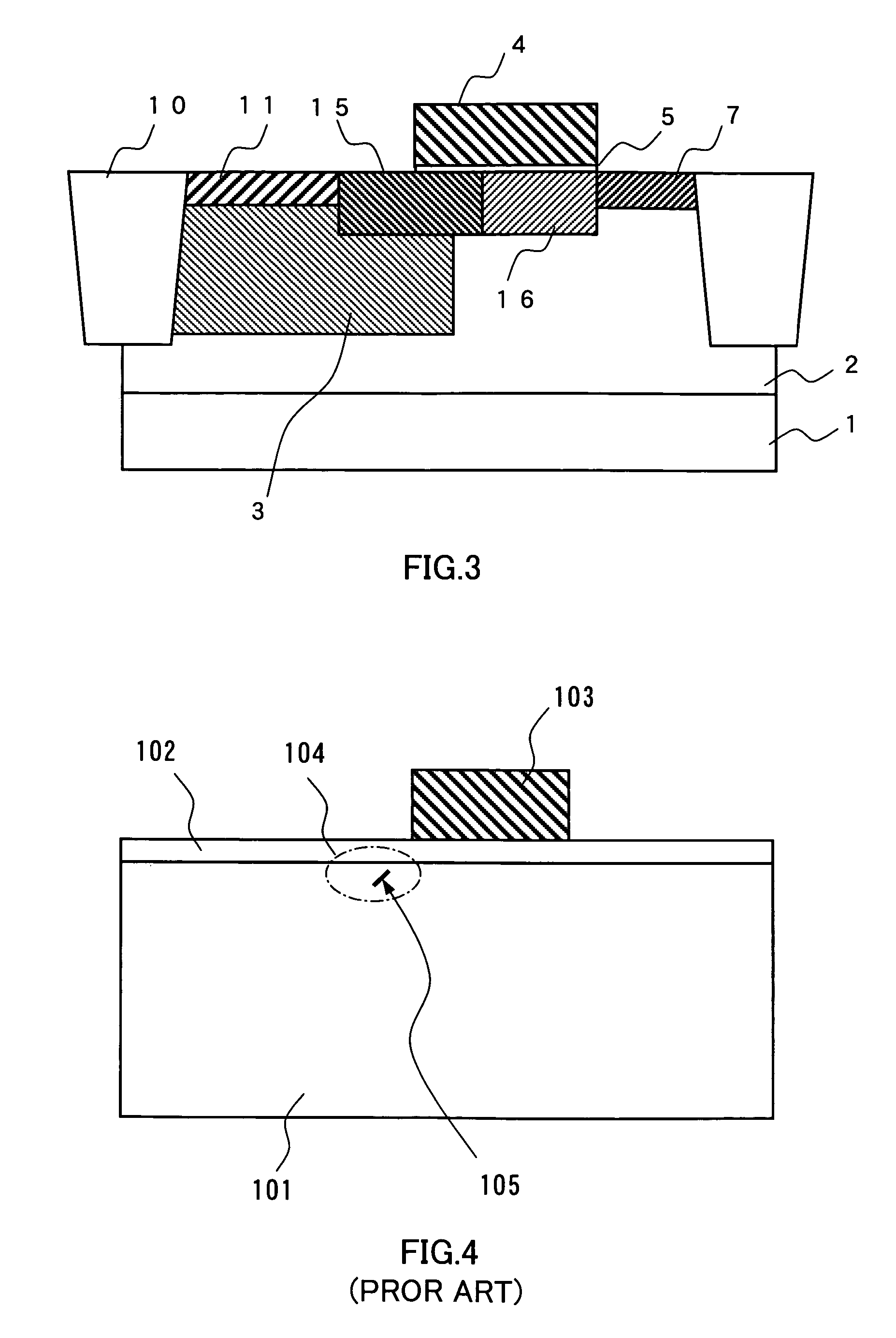
[0030]FIG. 3 is a cross-sectional view showing a cell structure of a solid-state imaging device according to a third embodiment. Identical reference numbers are used for components common to those of the first embodiment described above, and detailed explanation will be omitted for these components.

[0031]In this embodiment, a P-type second-B region 15 and a P-type third-A region 16 are formed in place of the P-type second region 12 and the P-type third region 13 of the first embodiment. This embodiment is characterized in that bottoms of the P-type diffusion layers of the P-type second-B region 15 and of the P-type third-A region 16 are positioned deeper than the bottoms of the P-type first region 11. For obtaining this structure, the energy of ion implantation during formation of the P-type diffusion layers is increased so as to position the bottoms of the P-type diffusion layers of the P-type second-B region 15 and of the P-type third A region 16 deeper than the ...


PUM


Abstract

A solid-state imaging device includes: a plurality of N-type photodiode regions formed inside a P-type well; a gate electrode having one edge being positioned adjacent to each of the photodiode regions; a N-type drain region positioned adjacent to the other edge of the gate electrode; an element-isolating portion having a STI structure, and a gate oxide film having a thickness of not more than 10 nm. One edge of the gate electrode overlaps the photodiode region. First, second and third regions are formed on a surface portion extending from the photodiode region to the drain region, in conditions such that the first region is disposed with a predetermined distance from one edge of the gate electrode and has a P-type first concentration C1, the second region is disposed with one edge positioned adjacent to the first region and the other edge overlapping the gate electrode and has a P-type second concentration C2, and the third region is disposed with one edge positioned adjacent to the second region and the other edge positioned adjacent to the drain region and has a P-type third concentration C3, wherein C1>C2>C3 or C1≈C2>C3. The readout characteristic at a low voltage is satisfactory, and image defects such as white flaws and dark current are suppressed sufficiently.

Description

FIELD OF THE INVENTION[0001]The present invention relates to a solid-state imaging device that uses an active MOS sensor. Particularly, the present invention relates to a solid-state imaging device that enables readout at a low voltage and suppresses image defects (especially for example, white flaws and dark current).BACKGROUND OF THE INVENTION[0002]A solid-state imaging device using an active MOS sensor is configured such that a signal detected by a photodiode is amplified at a transistor in each pixel, and the solid-state imaging device is characterized by its high sensitivity. A most serious problem for the solid-state imaging device is a reverse-direction leakage current at a pn junction of a silicon semiconductor. This leakage current, which cannot be isolated from a signal current generated by incident light, becomes a noise and degrades the performance of the solid-state imaging device. This leakage current is caused in part by stress applied to the silicon substrate.[0003]F...

Claims


Application Information

Patent Timeline
Patent Type & Authority Patents(United States)
IPC IPC(8): H01L31/062H01L31/113H01L27/146H01L31/10H04N5/335H04N5/367H04N5/369H04N5/374
CPCH01L27/14601H01L27/14609H01L27/1463H01L27/146H01L31/10
Inventor MIMURO, KENUCHIDA, MIKIYAOCHI, MOTOTAKA
Owner COLLABO INNOVATIONS INC
Why Eureka
Try Eureka