Semiconductor device having MIM structure resistor

a technology of resistor and semiconductor, which is applied in the direction of resistor, solid-state device, basic electric element, etc., can solve the problems of resistor being impossible to be used in the higher frequency range, capacitive interference of resistor with grounding interconnect, etc., and achieve the effect of improving high frequency characteristics

Active Publication Date: 2005-04-21
RENESAS ELECTRONICS CORP
View PDF2 Cites 58 Cited by
  • Summary
  • Abstract
  • Description
  • Claims
  • Application Information

AI Technical Summary

Benefits of technology

[0007] The present invention has been conceived to solve the foregoing problem incidental to the prior art. There is provided a semiconductor device including a resistor and a capacitor having MIM structure mounted therein, and having improved high frequency characteristics.
[0013] According to the semiconductor device of the present invention as described above, the capacitor having MIM structure is formed simultaneously with forming the resistor structure having MIM structure, and after providing a floating potential to the lower electrode of the resistor structure, the upper electrode is utilized to form a resistor. Thus, since the lower electrode of the resistor structure is a floating electrode, adverse effects of causing the parasitic capacitance in the resistor can be inhibited, thereby providing improved high frequency characteristics.

Problems solved by technology

Further, a grounding interconnects are provided in the lower part of the resistor, sandwiching the insulating film, and thus a capacitive interference thereof with the grounding interconnects may possibly be caused.
Therefore, such configuration may induce a considerable level of the parasitic capacitance between the resistor and the underlying interconnect, particularly in a higher frequency range, causing the resistor being impossible to be used in the higher frequency range.

Method used


Image

  • Semiconductor device having MIM structure resistor
  • Semiconductor device having MIM structure resistor
  • Semiconductor device having MIM structure resistor

Examples


first embodiment

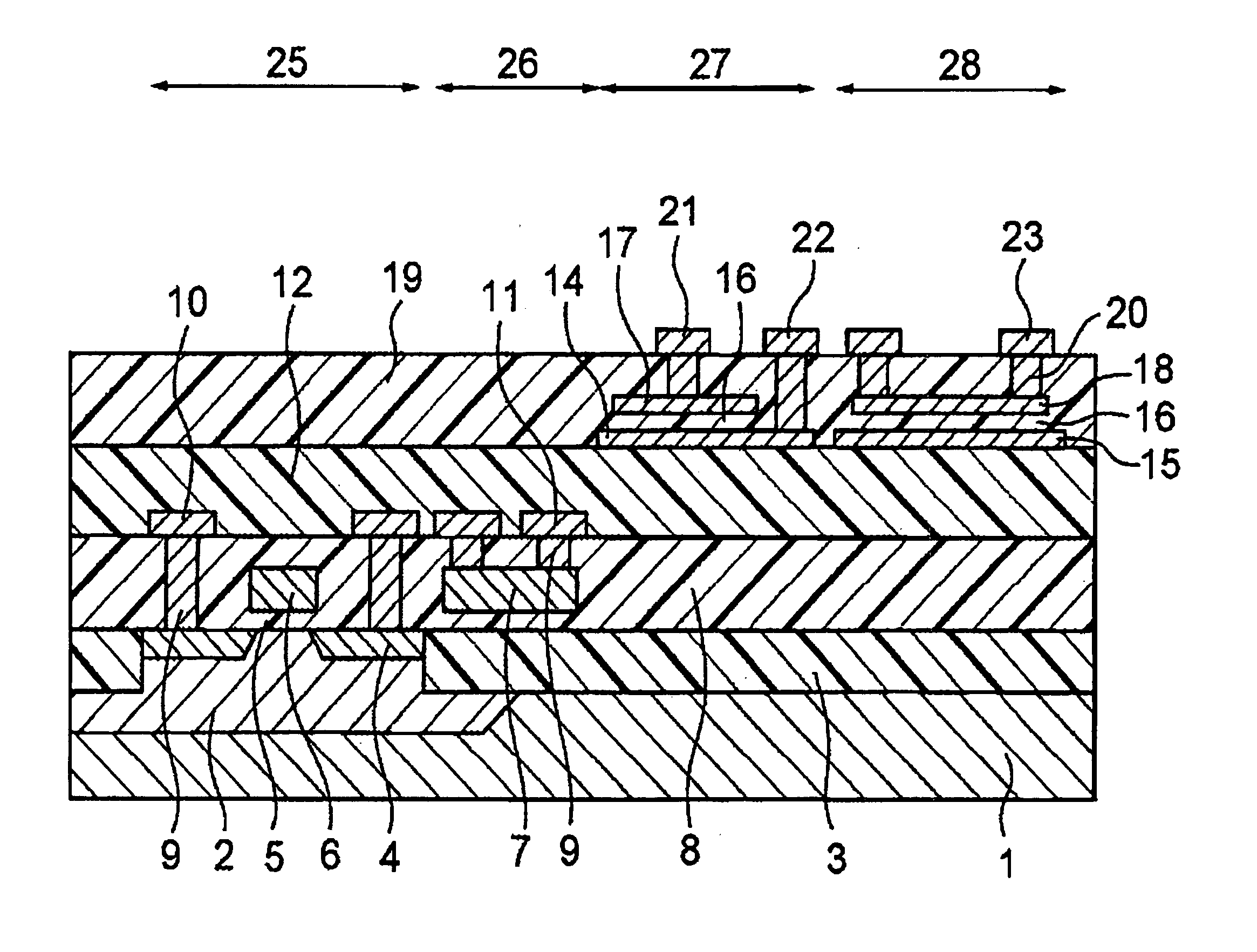
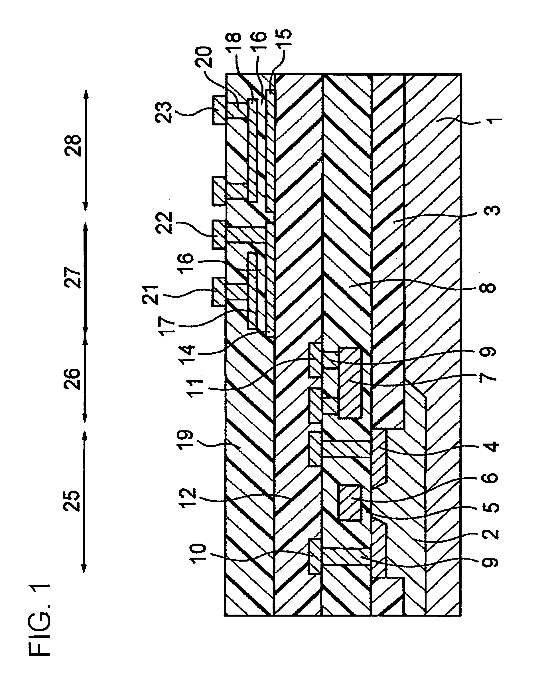
[0026] The first embodiment of the present invention will be described in reference to FIG. 1. In the first embodiment, a capacitor having MIM structure comprises a lower electrode (a metal lower electrode), a capacitive insulating film (a dielectric) and an upper electrode (a metal upper electrode), all of which are sequentially formed in this sequence. A resistor structure having MIM structure also comprises a lower electrode, a capacitive insulating film and a resistor, all of which are sequentially formed in this sequence. Here, in both structures, the lower electrode and the upper electrode are formed so that the lower electrode two-dimensionally includes the upper electrode. This is because the concern about causing the reliability problem is arisen when the multi-layered films comprising the lower electrode, the capacitive insulating film and the upper electrode, all of which are sequentially formed in this sequence, are simultaneously processed to have a common single patter...

second embodiment

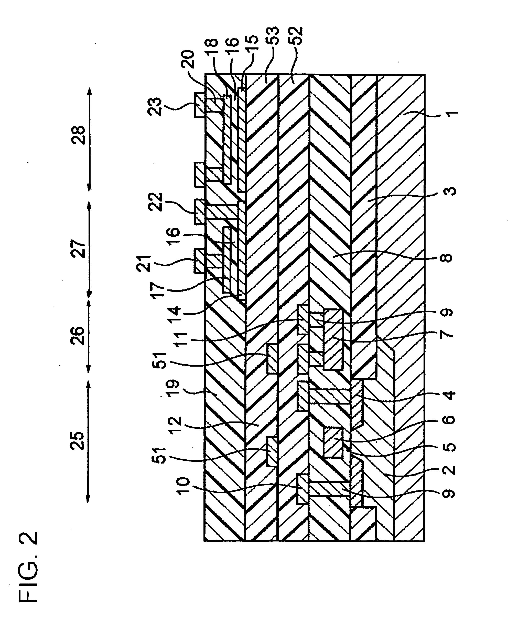
[0040] In the first embodiment, it has been illustrated that the MIM structure resistor has the two-dimensional geometries of the lower electrode and the upper electrode, which are different from that of the MIM structure capacitor. Therefore, two photo resist process steps are required for forming the lower electrode and the upper electrode of the MIM structure resistor and the MIM structure capacitor. Further, since the upper electrode and the lower electrode of the MIM structure capacitor are not symmetric, asymmetry may be generated, which, in turn, changes the characteristics thereof depending upon the manner of biasing the upper and the lower electrodes. On the contrary, since the second embodiment provides that each of the MIM structure resistor and the MIM structure capacitor has a single common two-dimensional geometry of the lower electrode and the upper electrode, the number of manufacturing process steps can be reduced to provide lower manufacturing cost, aside from the ...


PUM


Abstract

As for the resistor on the semiconductor substrate, it is required to achieve obtaining a metal resistor, which can be formed in the latter half of a preliminary process for manufacturing a semiconductor, in addition to forming a polysilicon resistor, which is formed in the first half of the preliminary process. A capacitor having MIM structure includes a lower electrode, a capacitive insulating film and an upper electrode, all of which are sequentially formed in this sequence. A resistor structure having MIM structure also includes a lower electrode, a capacitive insulating film and a resistor, all of which are sequentially formed in this sequence. In this case, the biasing conditions thereof should be selected so that the resistor structure lower electrode of the MIM structure resistor is not coupled to any electric potential, and is in a floating condition.

Description

[0001] This application is based on Japanese patent application No.2003-357877 and Japanese patent application No.2004-244321, the contents of which are incorporated hereinto by reference. BACKGROUND OF THE INVENTION [0002] 1. Field of the Invention [0003] The present invention relates to a semiconductor device, and particularly relates to a semiconductor device, which contains a capacitor and a resistor having metal-insulator-metal (MIM) structure. [0004] 2. Description of the Related Art [0005] Resistors are frequently employed as passive elements in semiconductor integrated circuits. In particular, besides the diffused resistor formed in the semiconductor substrate, a polysilicon film and a metal film are deposited on an insulating film that covers the semiconductor substrate and patterned to form a structure, which can be employed as a resistor. In the case of the polysilicon resistor, the resistor is often formed simultaneously with forming the gate electrode of the transistor ...

Claims


Application Information

Patent Timeline
Patent Type & Authority Applications(United States)
IPC IPC(8): H01L21/02H01L21/822H01L27/04H01L21/8234H01L27/06H01L27/088
CPCH01L27/0629H01L28/40H01L28/20H01L27/0688
Inventor KIKUTA, KUNIKONAKAYAMA, MAKOTO
Owner RENESAS ELECTRONICS CORP
Why Eureka
Try Eureka