DSP (digital signal processing) architecture with a wide memory bandwidth and a memory mapping method thereof

a technology of dsp and memory bandwidth, applied in the direction of architecture with multiple processing units, instruments, computation using denominational number representation, etc., can solve the problem of difficult processing of high-resolution images, and achieve the effects of reducing memory access times, high date rate, and high resolution

Inactive Publication Date: 2005-04-21
SAMSUNG ELECTRONICS CO LTD
View PDF9 Cites 43 Cited by
  • Summary
  • Abstract
  • Description
  • Claims
  • Application Information

AI Technical Summary

Benefits of technology

[0023] Therefore, according to the embodiments of the present invention, since a wide memory bandwidth is provided between a calculation element of the DSP architecture and a mem

Problems solved by technology

Therefore, it is difficult to process high resolution images due to the existence of

Method used


Image

  • DSP (digital signal processing) architecture with a wide memory bandwidth and a memory mapping method thereof
  • DSP (digital signal processing) architecture with a wide memory bandwidth and a memory mapping method thereof
  • DSP (digital signal processing) architecture with a wide memory bandwidth and a memory mapping method thereof

Examples


Embodiment Construction

[0032] Reference will now be made in detail to the embodiments of the present invention, examples of which are illustrated in the accompanying drawings, wherein like reference numerals refer to the like elements throughout. The embodiments are described below in order to explain the present invention by referring to the figures.

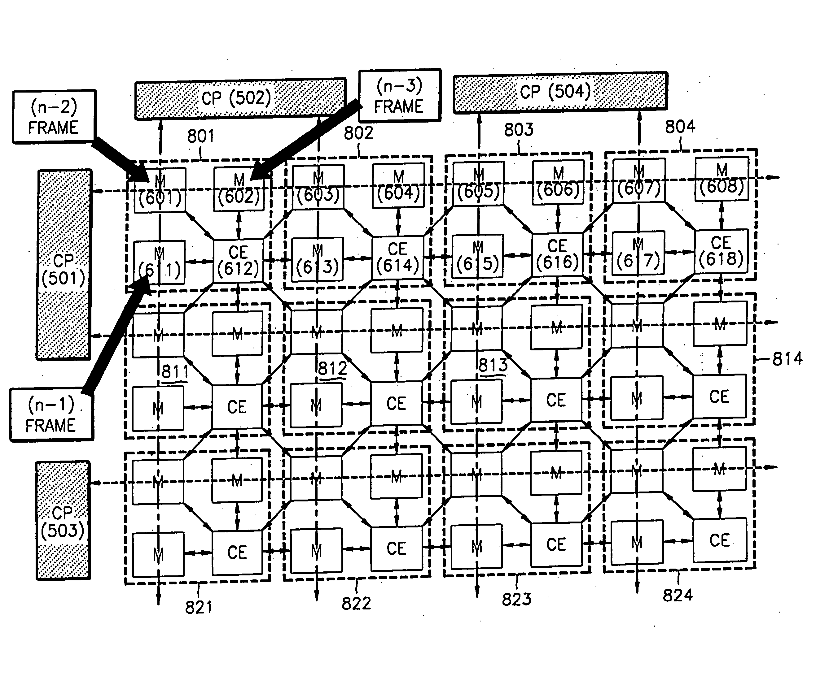
[0033]FIG. 3 illustrates a DSP (Digital Signal Processing) architecture 500 with a parallel structure, according to an embodiment of the present invention. Referring to FIG. 3, the DSP architecture 500 includes first and third communication ports (CPs) 501 and 503 arranged in a column direction and second and fourth communication ports (CPs) 502 and 504 arranged in a row direction. The first through fourth communication ports 501, 502, 503, and 504 are input / output ports to receive and / or transmit data from / to the DSP architecture 500. The first and the second communication ports 501 and 502 and the third and the fourth communication ports 503 and 504 are co...


PUM


Abstract

A DSP (Digital Signal Processing) architecture with a wide memory bandwidth and a memory mapping method thereof. The DSP architecture includes: a first communication port; first, second, and third memory devices, which are connected with the first communication port and are arranged in a first row direction of the DSP architecture; a fourth memory device, a calculation element, and a fifth memory device, which are arranged in a second row direction below a first row direction of the DSP architecture; and sixth, seventh, and eighth memory devices, which are connected with the first communication port and arranged in a third row direction of the DSP architecture, wherein the calculation element is connected with the first through the eight memory devices. In the DSP architecture, the calculation element and the first through the eighth memory devices form one arrangement unit, wherein the calculation element is disposed in the center of the arrangement unit, the first through the eighth memory devices are connected to the calculation element, and a plurality of arrangement units are arranged in row directions and column directions of the DSP architecture. Therefore, since a wide data bandwidth is provided between the calculation element of the DSP architecture and the memory devices, it is possible to reduce memory access times when data is processed, and accordingly, to process data with a high data rate, such as a moving image with a high resolution.

Description

CROSS-REFERENCE TO RELATED APPLICATIONS [0001] This application claims the priority of Korean Patent Application No. 2003-58781, filed on Aug. 25, 2003, in the Korean Intellectual Property Office, the disclosure of which is incorporated herein in its entirety by reference. BACKGROUND OF THE INVENTION [0002] 1. Field of the Invention [0003] The present invention relates to a DSP (digital signal processing) architecture, and more particularly, to a DSP architecture that provides a wide memory bandwidth according to an image processing algorithm, and a memory mapping method thereof. [0004] 2. Description of the Related Art [0005] One among basic functions that are performed by a digital processor is to access a memory for data reading and writing. The memory is generally accessed by an address provided from a digital processor. The memory access operation of the digital processor is greatly influenced by the input-output structure of the memory, and particularly, is closely related to ...

Claims


Application Information

Patent Timeline
IPC IPC(8): G06F13/00G06F12/00
CPCG06F15/8023G06F12/00
Inventor YUN, HYUN-KYUKWAK, HAN-TAK
Owner SAMSUNG ELECTRONICS CO LTD
Why Eureka
Try Eureka