Dielectric thermal stack for the cooling of high power electronics

a technology of dielectric thermal stack and high-power electronics, which is applied in the direction of cooling/ventilation/heating modification, semiconductor device details, semiconductor/solid-state device details, etc., can solve the problems of junction temperature rising to a level where the device fails to function, devices and interconnects may also fail, and the device and interconnect may also fail. to achieve the effect of improving heat transfer, increasing surface area and increasing surface area

Inactive Publication Date: 2005-04-21
VISTEON GLOBAL TECH INC
View PDF25 Cites 62 Cited by
  • Summary
  • Abstract
  • Description
  • Claims
  • Application Information

AI Technical Summary

Benefits of technology

[0008] In yet another aspect of the invention, the outer wall of the chamber includes fins that increase the surface area thereby improving the heat transfer between the outer wall and the second fluid. Further, the fins may include a porous material, such as graphite or metal foam, to further increase the surface area and improve heat transfer between the chamber and second fluid.

Problems solved by technology

These thermal losses can adversely affect the performance and reliability of the device by causing the device to overheat.
When the device overheats, the junction temperature rises to a level where the device fails to function.
In addition, the devices and interconnects may also fail due to thermal expansion effects, as a mismatch in thermal expansion characteristics can cause solder joint cracking.

Method used


Image

  • Dielectric thermal stack for the cooling of high power electronics
  • Dielectric thermal stack for the cooling of high power electronics
  • Dielectric thermal stack for the cooling of high power electronics

Examples


Embodiment Construction

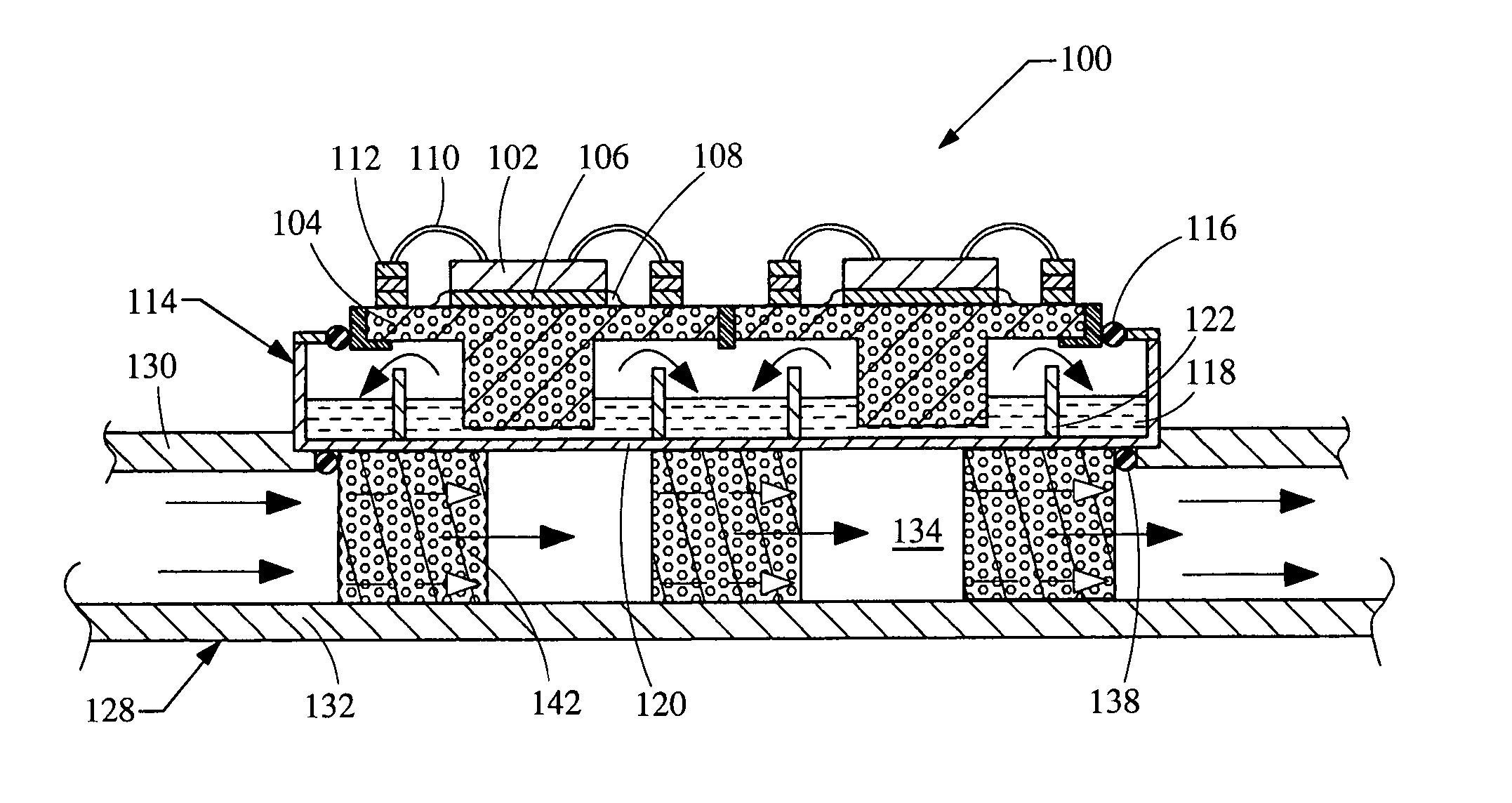
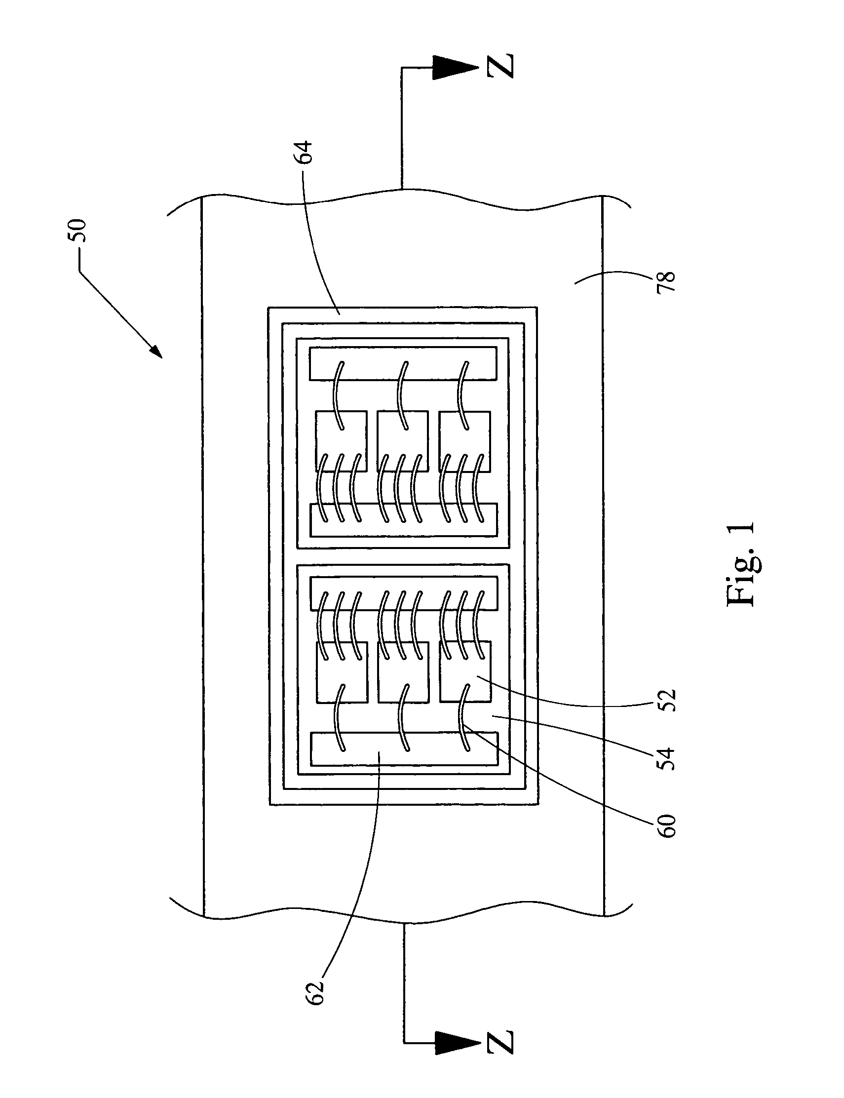
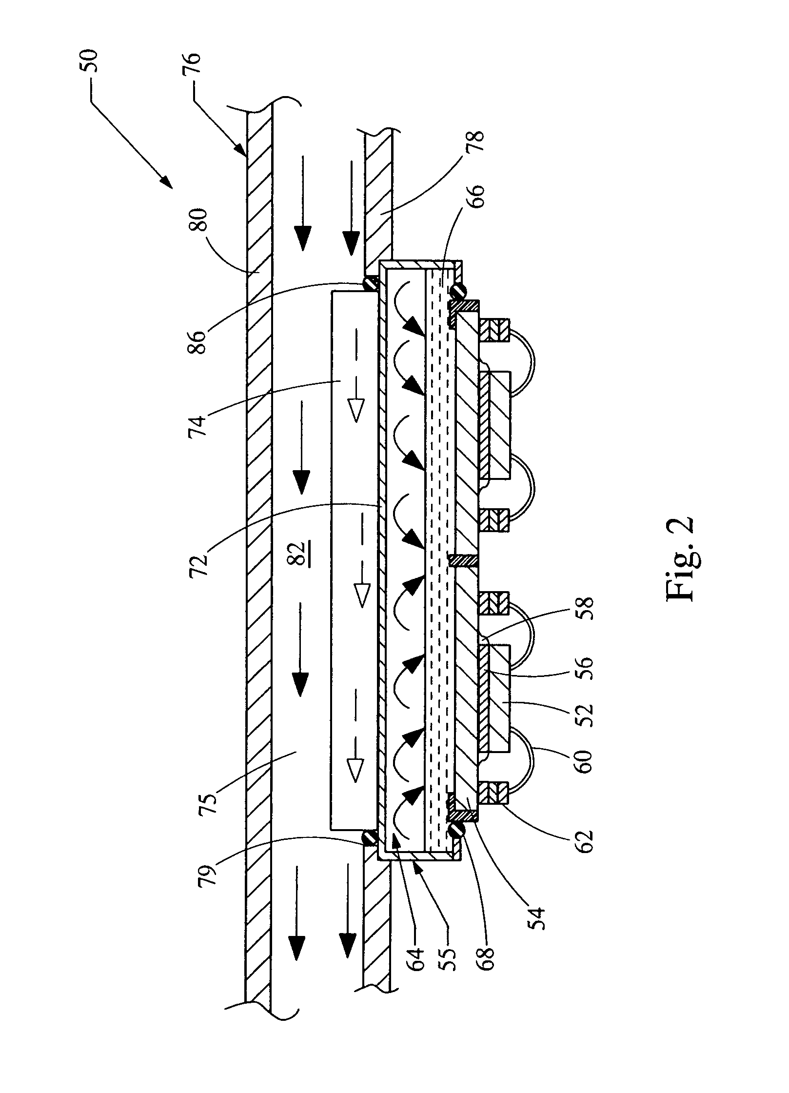
[0017] Referring now to FIGS. 1 and 2, a system embodying the principles of the present invention is illustrated therein and generally designated at 50. The system 50 includes a die 52, a substrate 54, heat sink 55 containing a first fluid and a base 76 containing a second fluid 82.

[0018] The die 52 is electrically connected to bond pads 62 formed on the substrate 54 through the wire bonds 60. The die 52 is thermally connected to the substrate 54 using a phase changing or liquefiable solder 56. Alternatively, this thermal connection may be made through more common solder or thermally conductive adhesive. When phase changing solder 56 is used, a sealant 58 is attached between the die 52 and the substrate 54 and configured to encapsulate the liquefiable solder 56. However, other more common attachment techniques may be used. The substrate 54 is made of a material with good thermal conductivity. Metal, specifically copper, is an example of an appropriate material for the substrate 54....


PUM


Abstract

A system for dissipating heat in an electronic power module is provided. The system includes a semiconductor die, a substrate, and a heat sink in which is contained a first fluid, and a conduit through which a second fluid is permitted to flow. The substrate is attached on one surface to the die and configured to conduct heat from the die. The heat sink is attached to another surface of the substrate and transfers heat from the die to the first fluid contained therein, which evaporates due to the heat provided by the substrate. The fluid is condensed on a condensing wall cooled by the second fluid, which flows across the outer surface of the condensing wall, to transport heat away from the heat sink.

Description

BACKGROUND [0001] 1. Field of the Invention [0002] The present invention generally relates to the dissipation of heat from a power module. More specifically, the invention relates to the dissipation of heat from a power module utilizing a vapor fluid heat sink. [0003] 2. Description of Related Art [0004] In high power electronic applications, such as those used in electrical vehicle designs, a significant amount of heat is generated in semiconductor devices that control the switching of power. These thermal losses can adversely affect the performance and reliability of the device by causing the device to overheat. When the device overheats, the junction temperature rises to a level where the device fails to function. In addition, the devices and interconnects may also fail due to thermal expansion effects, as a mismatch in thermal expansion characteristics can cause solder joint cracking. Therefore, it is advantageous to maximize the capability of heat dissipation and to minimize th...

Claims


Application Information

Patent Timeline
Patent Type & Authority Applications(United States)
IPC IPC(8): H01L23/373H01L23/427H01L23/473H05K7/20
CPCH01L23/3733H01L23/427H01L23/473H01L2224/48091H01L2224/49111H01L2224/73265H01L2224/49175H01L2924/00014H01L2224/49113
Inventor JAIRAZBHOY, VIVEKREDDY, PRATHAP A.PARUCHURI, MOHANBAKER, JAY D.
Owner VISTEON GLOBAL TECH INC
Why Eureka
Try Eureka