Method for fabricating a double gate MOSFET device

a transistor device and finfet technology, applied in the direction of transistors, semiconductor devices, electrical devices, etc., can solve the problems of increasing the difficulty of further scaling of the planar structure below 50 nm, and achieve the effect of preventing the phenomenon of gate depletion, excellent short channel behavior, and better gate control

Inactive Publication Date: 2005-04-28
UNITED MICROELECTRONICS CORP
View PDF17 Cites 30 Cited by
  • Summary
  • Abstract
  • Description
  • Claims
  • Application Information

AI Technical Summary

Benefits of technology

[0009] It is one objective of the present invention to provide a method of fabricating a double gate MOSFET device, which can prevent depletion of a polysilicon gate by improving the distributed uniformity of dopants in the polysilicon gate.
[0010] It is another objective of the present invention to provide a method of fabricating a double gate MOSFET device, which reduces the short channel effect and has a better gate control.
[0012] The recess structures under the channel regions make the topography of the conductive gate layer significantly deviating from a plain profile. As a consequence, a more uniformly distributed doped conductive gate layer can be obtained by performing the titled ion implantation due to the topography of the conductive gate layer. A gate depletion phenomenon is thus prevented upon operating the double gate MOSFET device. Furthermore, an excellent short channel behavior and a better gate control are achieved by the double gate structure of the present invention.

Problems solved by technology

However, further scaling of the planar structure below 50 nm becomes increasingly challenging due to excess leakage, degradation in mobility, and a variety of difficulties within the device processing.

Method used


Image

  • Method for fabricating a double gate MOSFET device
  • Method for fabricating a double gate MOSFET device
  • Method for fabricating a double gate MOSFET device

Examples


Embodiment Construction

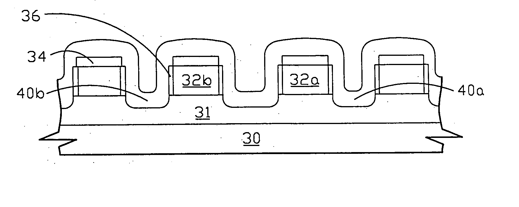
[0018] Referring now to the drawing of FIG. 4, which illustrates a schematic partial perspective view of a double gate MOSFET device provided by the present invention. In the present invention, the double gate MOSFET device is fabricated on an insulating layer, for example, a buried oxide layer (BOX) 31, overlying a semiconductor substrate 30, and includes a silicon source region 32c and a silicon drain region 32d connected by a silicon fin or channel. Hence, the double gate MOSFET device includes FinFET transistors. The source region 32c, drain region 32d and the channel are covered by a cap oxide layer 34. A gate 40a straddles the channel fin and perpendicular to the source region 32c and the drain region 32d and is isolated thereon by gate oxide and the cap oxide layer 34. Thus, inversion layers are formed on both vertical sidewalls of the channel. A recess structure is formed under each sidewall of the channel. The structure of the double gate MOSFET device has advantages of pro...


PUM


Abstract

A method of fabricating a double gate MOSFET device is provided. The present invention overetches a silicon layer overlying a buried oxide layer using a hard mask of cap oxide on the silicon layer as an etching mask. As a result, source, drain and channel regions are formed extending from the buried oxide layer, and a pair of recesses are formed under the channel regions in the buried oxide layer. The channel is a fin structure with a top surface and two opposing parallelly sidewalls. The bottom recess is formed under each opposing sidewall of the fin structure. A conductive gate layer is formed straddling the fin structures. The topography of the conductive gate layer significantly deviates from the conventional plainer profile due to the bottom recess structures under the channel regions, and a more uniformly distributed doped conductive gate layer can be obtained. Hence, the depletion effect of the conductive polysilicon gate while operating the device can be suppressed and the device drive-on currents can be further enhanced.

Description

BACKGROUND OF THE INVENTION [0001] 1. Field of the Invention [0002] The present invention relates to a method for fabricating a FinFET transistor device, and more particularly to a method of fabricating a double gate MOSFET with a capability of inhibiting the depletion effect of the conductive gate while operating this device, which can hence elevate the device drive-on currents. [0003] 2. Description of the Prior Art [0004] In the past several years, significant progress has been made for the scaling of classical planar MOSFET (metal-oxide-semiconductor field effect transistor) structure to the gate lengths below 65 nm. Despite difficulties in fabrication, sub-20 nm physical gate length MOSFETs have recently been demonstrated. However, further scaling of the planar structure below 50 nm becomes increasingly challenging due to excess leakage, degradation in mobility, and a variety of difficulties within the device processing. Therefore, alternative MOSFET structures and new process ...

Claims


Application Information

Patent Timeline
Patent Type & Authority Applications(United States)
IPC IPC(8): H01L21/336H01L29/423H01L29/49H01L29/786
CPCH01L29/42384H01L29/4908H01L29/785H01L29/66803H01L29/66795
Inventor LIAO, WEN-SHIANGSHIAU, WEI-TSUN
Owner UNITED MICROELECTRONICS CORP
Why Eureka
Try Eureka