Charge pump circuit having high charge transfer efficiency

Inactive Publication Date: 2005-04-28
SAMSUNG ELECTRONICS CO LTD
View PDF6 Cites 20 Cited by
  • Summary
  • Abstract
  • Description
  • Claims
  • Application Information

AI Technical Summary

Benefits of technology

[0014] The present invention provides a charge pump circuit that improves the charge transfer efficiency of a charge t

Problems solved by technology

Recent reductions in the power supply voltage provided to chips make it difficult to generate a high

Method used


Image

  • Charge pump circuit having high charge transfer efficiency
  • Charge pump circuit having high charge transfer efficiency
  • Charge pump circuit having high charge transfer efficiency

Examples


Embodiment Construction

[0023] The present invention will now be described more fully with reference to the accompanying drawings, in which an embodiment of the invention is shown. Throughout the drawings, like reference numerals are used to refer to like elements.

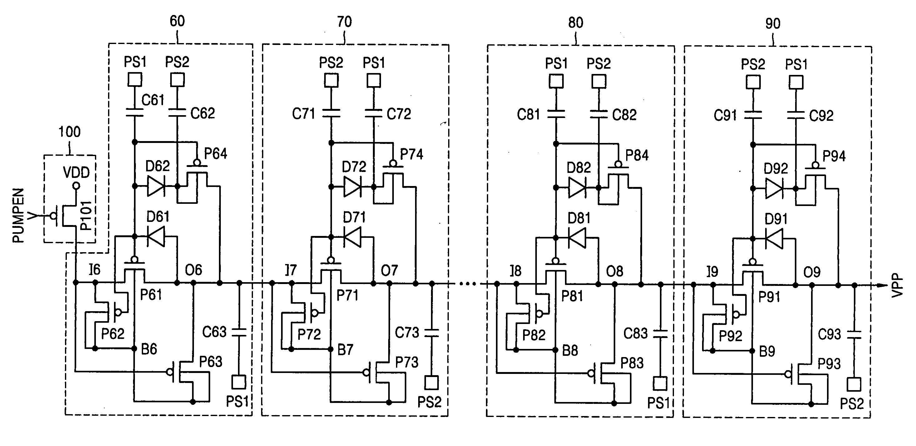
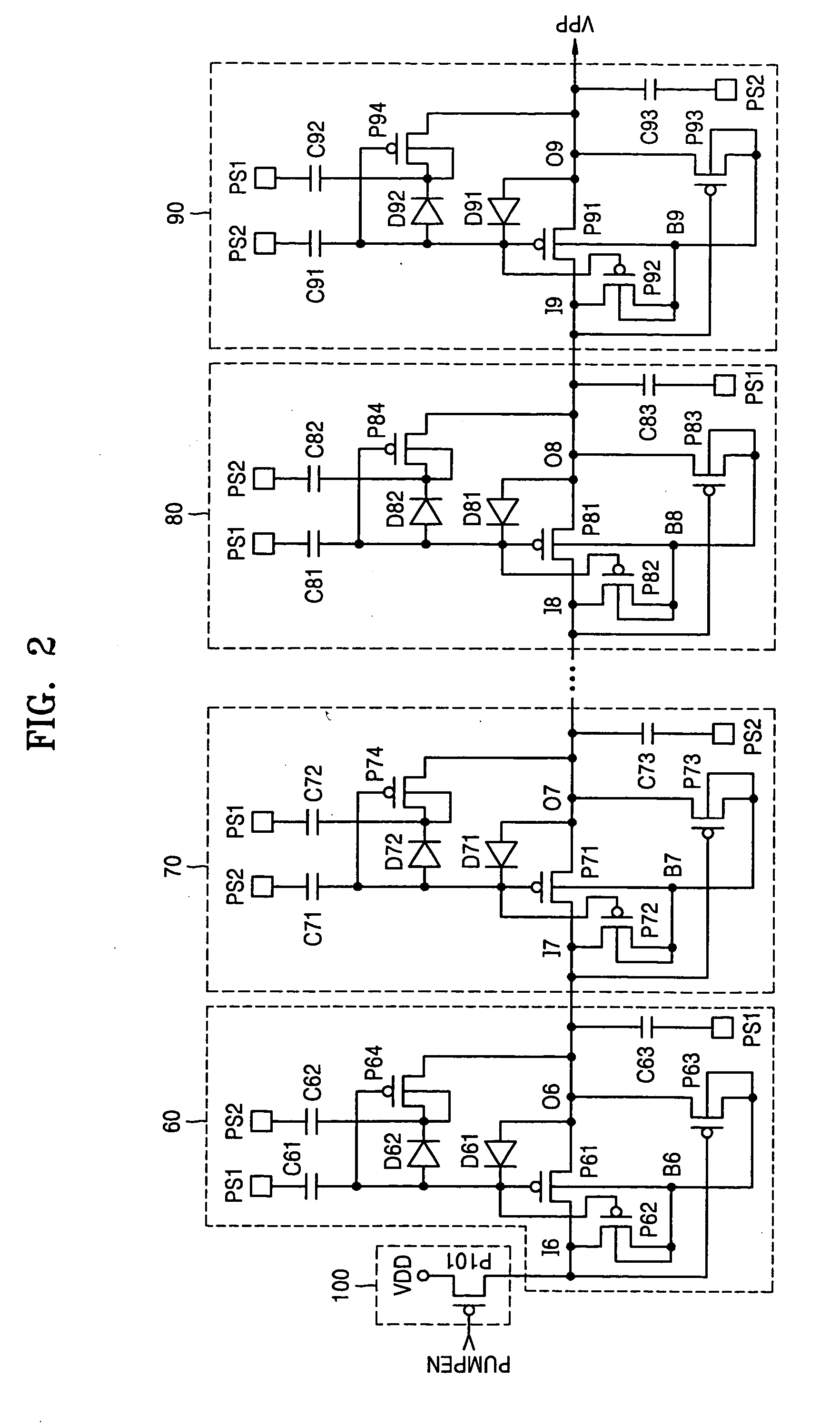
[0024]FIG. 2 is a circuit diagram of a charge pump circuit according to an embodiment of the present invention.

[0025] Referring to FIG. 2, the charge pump circuit includes a charge supply unit 100 and a plurality of boosting stages 60, 70, 80, and 90 that are connected in series.

[0026] The charge supply unit 100 supplies charges to an input node I6 of the first boosting stage 60 among the plurality of boosting stages 60, 70, 80, and 90 in response to an enable signal PUMPEN. The charge supply unit 100 includes a PMOS transistor P101. A power supply voltage VDD is provided to the source of the PMOS transistor P101, an enable signal PUMPEN is provided to the gate of the PMOS transistor P101, and the drain of the PMOS transistor P101 is connected...


PUM


Abstract

A charge pump circuit alleviates the body effect of a charge transfer transistor, thereby improving the charge transfer efficiency of the charge transfer transistor and thus pumping efficiency. The charge pump circuit includes a plurality of boosting stages that have input nodes and boosting nodes that are connected in series. Each of the boosting stages includes a charge transfer transistor and a first switch transistor, their respective gates being connected together. A first terminal of the charge transfer transistor is connected to one of the input nodes, and a second terminal of the charge transfer transistor is connected to one of the boosting nodes. The first switch transistor makes the voltage level at the bulk of the charge transfer transistors equal to the voltage level at the first terminal of the charge transfer transistor while charges are being transferred through the charge transfer transistor.

Description

CROSS REFERENCE TO RELATED APPLICATION [0001] This application claims the priority of Korean Patent Application No. 2003-75225, filed on Oct. 27, 2003, in the Korean Intellectual Property Office, the disclosure of which is hereby incorporated by reference in its entirety. BACKGROUND OF THE INVENTION [0002] 1. Field of the Invention [0003] The present invention relates to a semiconductor integrated circuit, and more particularly, to a charge pump circuit. [0004] 2. Description of the Related Art [0005] In general, non-volatile memory devices that are erasable and programmable perform erase and programming operations on memory cells by using fowler-nordheim (F-N) tunneling or channel hot electron injection. To this end, a high voltage that is higher than a power supply voltage provided from the outside is required. The high voltage may be provided through an external pin or generated and used in a chip. To generate such a high voltage within a chip, a high voltage generating circuit i...

Claims


Application Information

Patent Timeline
IPC IPC(8): G05F3/02G11C16/06G11C16/30H02M3/07H03K17/06H03K17/687
CPCH02M3/073H03K2217/0018H02M2003/078H02M3/078G11C16/30
Inventor HAHN, WOOK-GHEEBYEON, DAE-SEOK
Owner SAMSUNG ELECTRONICS CO LTD
Why Eureka
Try Eureka