Semiconductor memory device of hierarchy word type and sub word driver circuit

a memory device and memory array technology, applied in the field of semiconductor memory devices, can solve the problems of increasing the number of wiring lines on the memory array, complicated circuit structure, and delay in non-selection of word lines, so as to reduce the number of wiring lines

Active Publication Date: 2005-04-28
LONGITUDE LICENSING LTD
View PDF8 Cites 3 Cited by
  • Summary
  • Abstract
  • Description
  • Claims
  • Application Information

AI Technical Summary

Benefits of technology

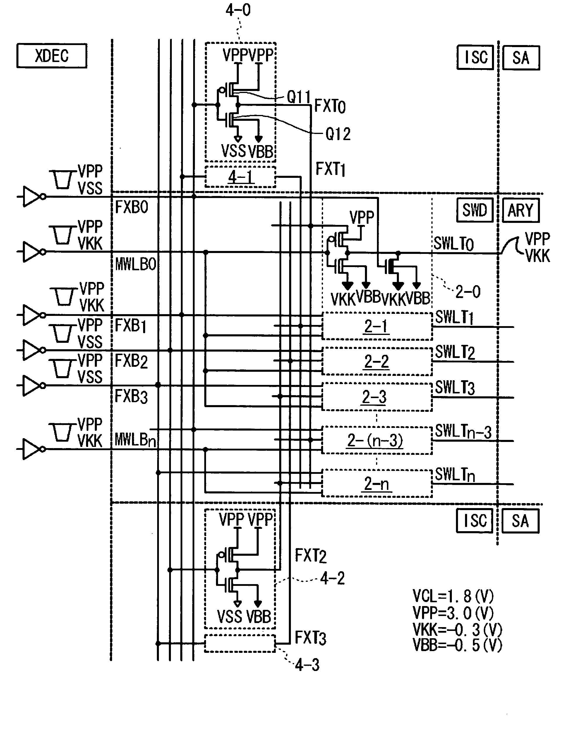
[0019] Therefore, an object of the present invention is to provide a semiconductor device that the number of wiring lines can be reduced which pass on a memory array, and a sub word driver used for the same.
[0020] Another object of the present invention is to provide a sub word circuit which can prevent a delay at the time of the non-selection of a word line.
[0022] Another object of the present invention is to provide a semiconductor device in which a consumption current in a negative voltage can be reduced without being accompanied by the increase of a manufacturing process, while being simply set to the negative voltage and a sub word driver used for the same.

Problems solved by technology

In a DRAM (dynamic random access memory) field as an example of a semiconductor memory device, increase of a memory capacity and finer processing go ahead every year and the circuit structure becomes complicated.
Therefore, a fault is sometimes incorporated in the manufacturing and design processes, but such a fault is screened by a simple test process.
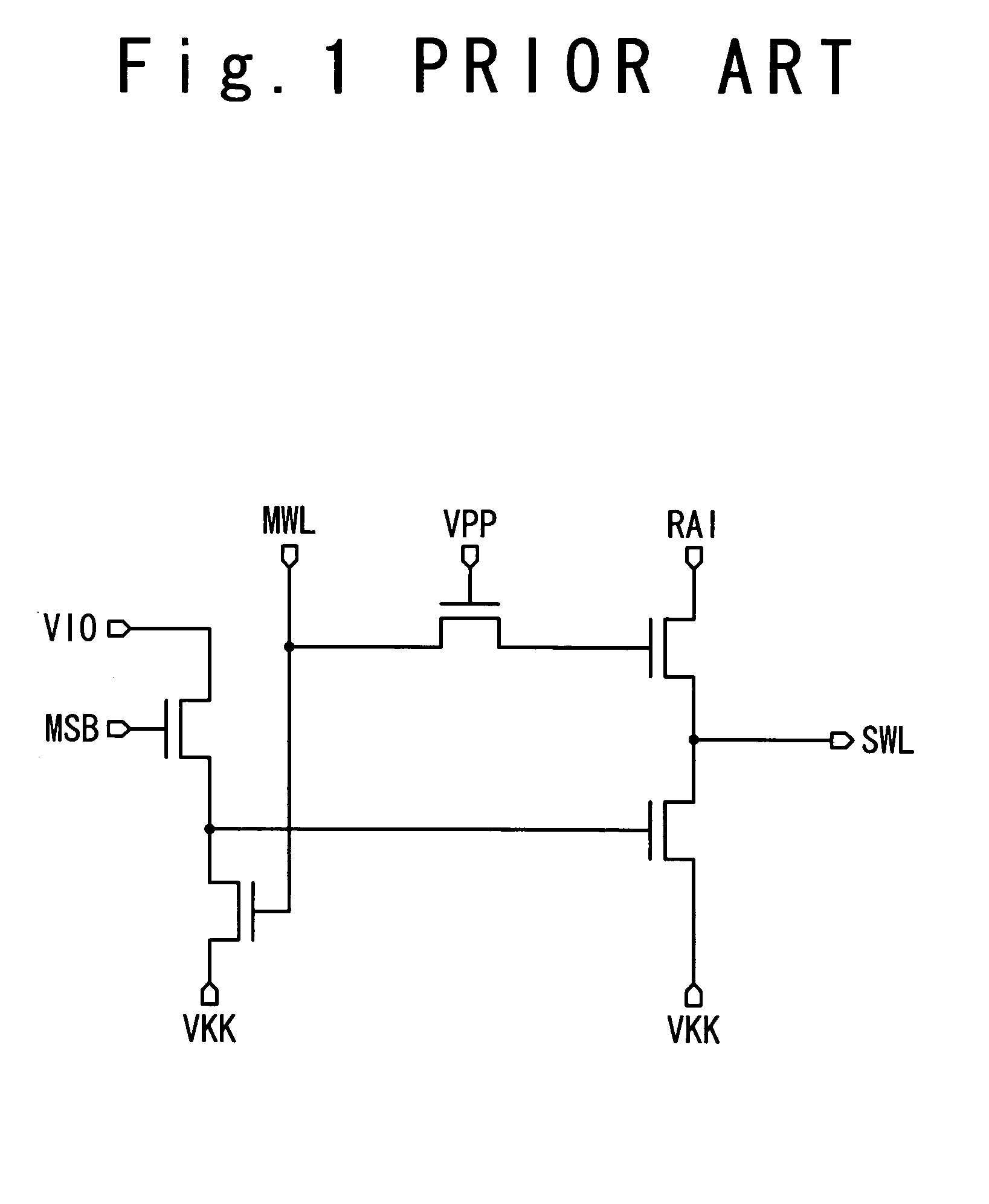
However, in this negative word system, because an MOS transistor with a high threshold voltage Vth is used as the N-type MOSFET selected in the non-selection of the word line, a delay is caused in the non-selection of the word line.
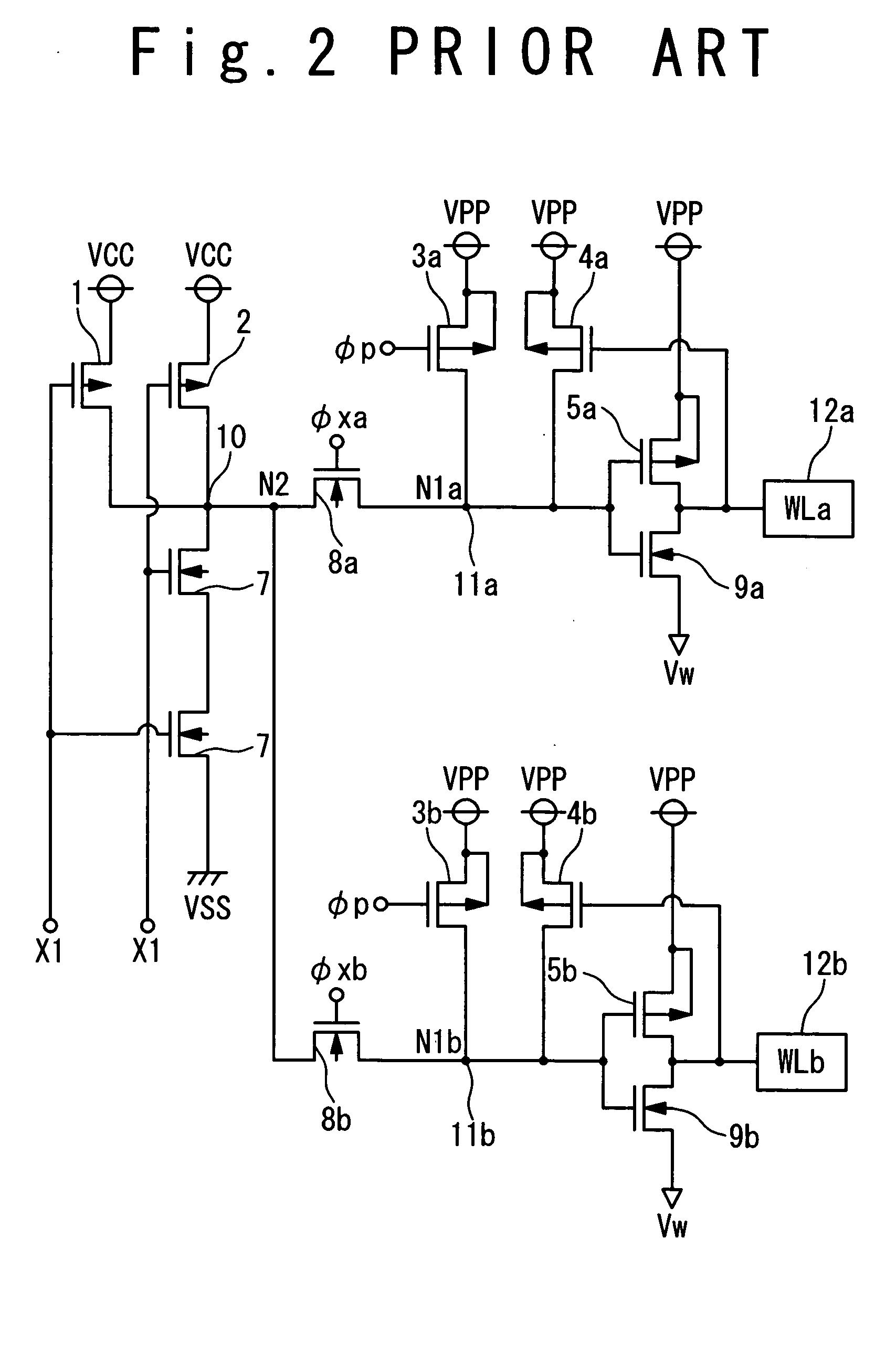
Therefore, the number of wiring lines on the memory array increases and the wiring line width cannot be widened.

Method used


Image

  • Semiconductor memory device of hierarchy word type and sub word driver circuit
  • Semiconductor memory device of hierarchy word type and sub word driver circuit
  • Semiconductor memory device of hierarchy word type and sub word driver circuit

Examples


Embodiment Construction

[0047] Hereinafter, a semiconductor device containing a semiconductor memory device with a sub word driver circuit of the present invention will be described with reference to the attached drawings. FIG. 5 shows the semiconductor memory device to which the sub word driver circuit of the present invention is applied. As shown in FIG. 5, the semiconductor memory device of the present invention has a memory cell array. The memory cell array has a plurality of banks (BANK), eight banks BANK0 to BANK7 in this example. One of the eight banks BANK0 to BANK7 is specified using a part of an address inputted to the semiconductor memory device. The remaining part of the address is supplied to a specified bank(s). Because this operation is known to a person in the art, the description is omitted.

[0048]FIG. 6 is a diagram showing a structure of each bank in the semiconductor memory device. As shown in FIG. 6, each bank has four sub arrays. A sub amplifier circuit section SUBAMP and an X decoder...


PUM


Abstract

In a sub word driver circuit in a semiconductor memory device of a hierarchy word structure using a main word line signal and a sub word line signal, a first NMOS transistor and a first PMOS transistor are connected in series. A second NMOS transistor is connected with a node between the first PMOS transistor and the first NMOS transistor. The source of the first PMOS transistor is connected with a sub word line inverted signal obtained by inverting the sub word line signal, and the source of the first NMOS transistor is connected with a first negative voltage. A single main word line signal is connected to a gate of the first PMOS transistor and a gate of the first NMOS transistor, and the sub word line signal is connected with a gate of the second NMOS transistor.

Description

BACKGROUND OF THE INVENTION [0001] 1. Field of the Invention [0002] The present invention relates to a semiconductor memory device, and more particularly to a sub word driver circuit used for a semiconductor memory device having a hierarchy word structure. [0003] 2. Description of the Related Art [0004] In a DRAM (dynamic random access memory) field as an example of a semiconductor memory device, increase of a memory capacity and finer processing go ahead every year and the circuit structure becomes complicated. Therefore, a fault is sometimes incorporated in the manufacturing and design processes, but such a fault is screened by a simple test process. It is effective in cost reduction to improve a refreshing characteristic, which is a basic characteristic of the DRAM, through the screening, in addition to the improvement of the whole chip characteristics. [0005] Under such a situation, it has been studied to decrease boron concentration in a memory cell transistor for improvement o...

Claims


Application Information

Patent Timeline
Patent Type & Authority Applications(United States)
IPC IPC(8): G11C8/08G11C11/407G11C8/14G11C11/401
CPCG11C8/14G11C8/08
Inventor DONO, CHIAKIKOSHIKAWA, YASUJI
Owner LONGITUDE LICENSING LTD
Why Eureka
Try Eureka