Surface-emitting semiconductor laser and method for manufacturing thereof as well as optical device

a semiconductor laser and surface-emitting technology, applied in the direction of laser details, laser optical resonator construction, optical resonator shape and construction, etc., can solve the problems of increasing the difficulty of high-order-mode leakage, reducing the effective refractive-index difference in size, and restricting the increase of q value, etc., to achieve enhanced light-emission efficiency, high power output, and large current

a semiconductor laser and surface-emitting technology, applied in the direction of laser details, laser optical resonator construction, optical resonator shape and construction, etc., can solve the problems of increasing the difficulty of high-order-mode leakage, reducing the effective refractive-index difference in size, and restricting the increase of q value, etc., to achieve enhanced light-emission efficiency, high power output, and large current

US20050089075A1Active Publication Date: 2005-04-28SONY CORP +1

Image

  • Surface-emitting semiconductor laser and method for manufacturing thereof as well as optical device
  • Surface-emitting semiconductor laser and method for manufacturing thereof as well as optical device
  • Surface-emitting semiconductor laser and method for manufacturing thereof as well as optical device

Examples


Embodiment Construction

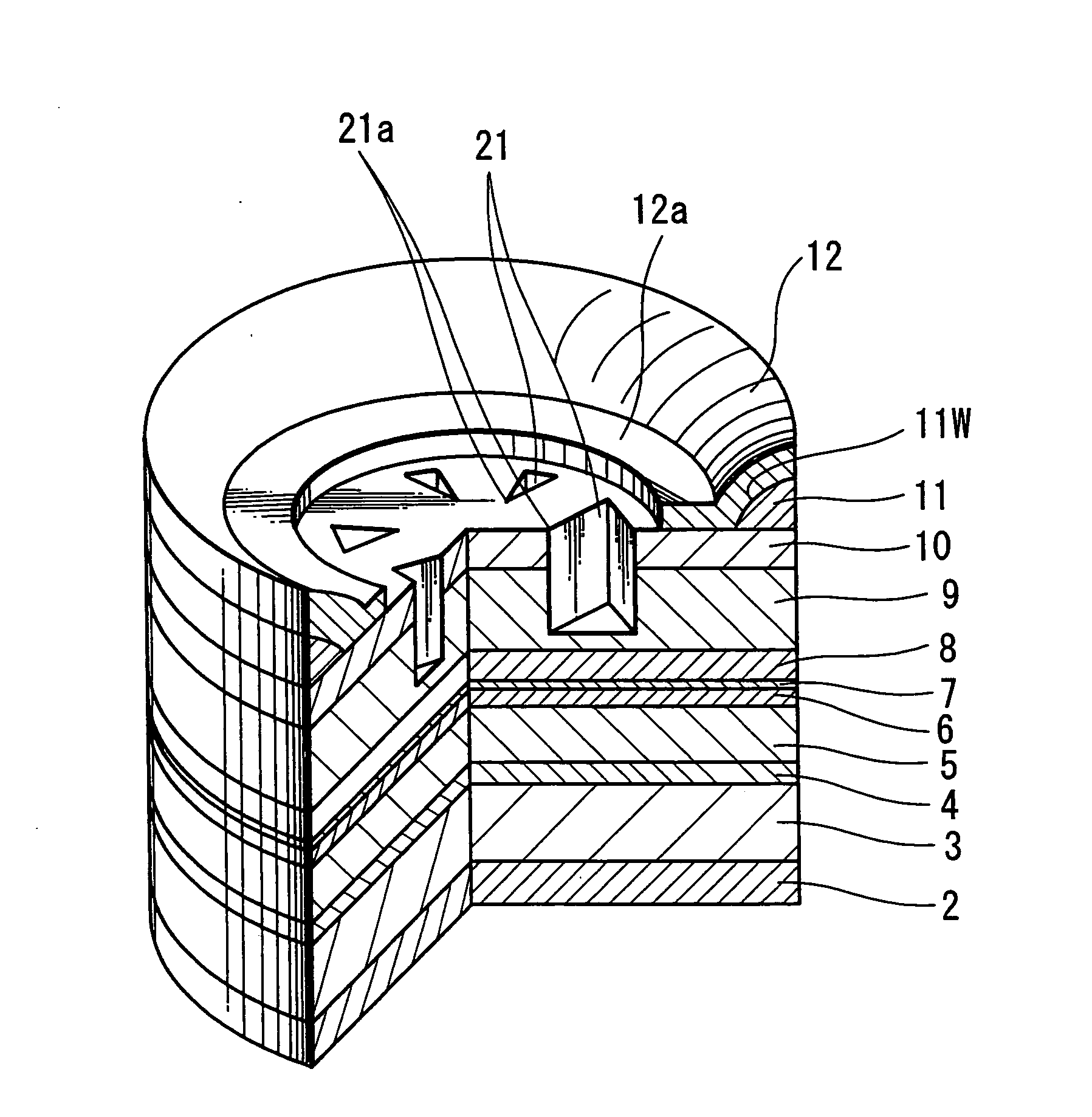
[0060] The present invention relates to a surface-emitting semiconductor laser and a method for manufacturing thereof as well as an optical device including a light-source device in which the surface-emitting semiconductor laser is used. In particular, the present invention relates to a surface-emitting semiconductor laser in which expansion of the mode-field diameter allows for an increase in output with maintaining a single horizontal mode and a method for manufacturing thereof as well as an optical device.

[0061] Various embodiments of a surface-emitting semiconductor laser and an optical device including a light-source device composed of a surface-emitting semiconductor laser will be described below as an illustrative example of the present invention and not limitative to the scope thereof.

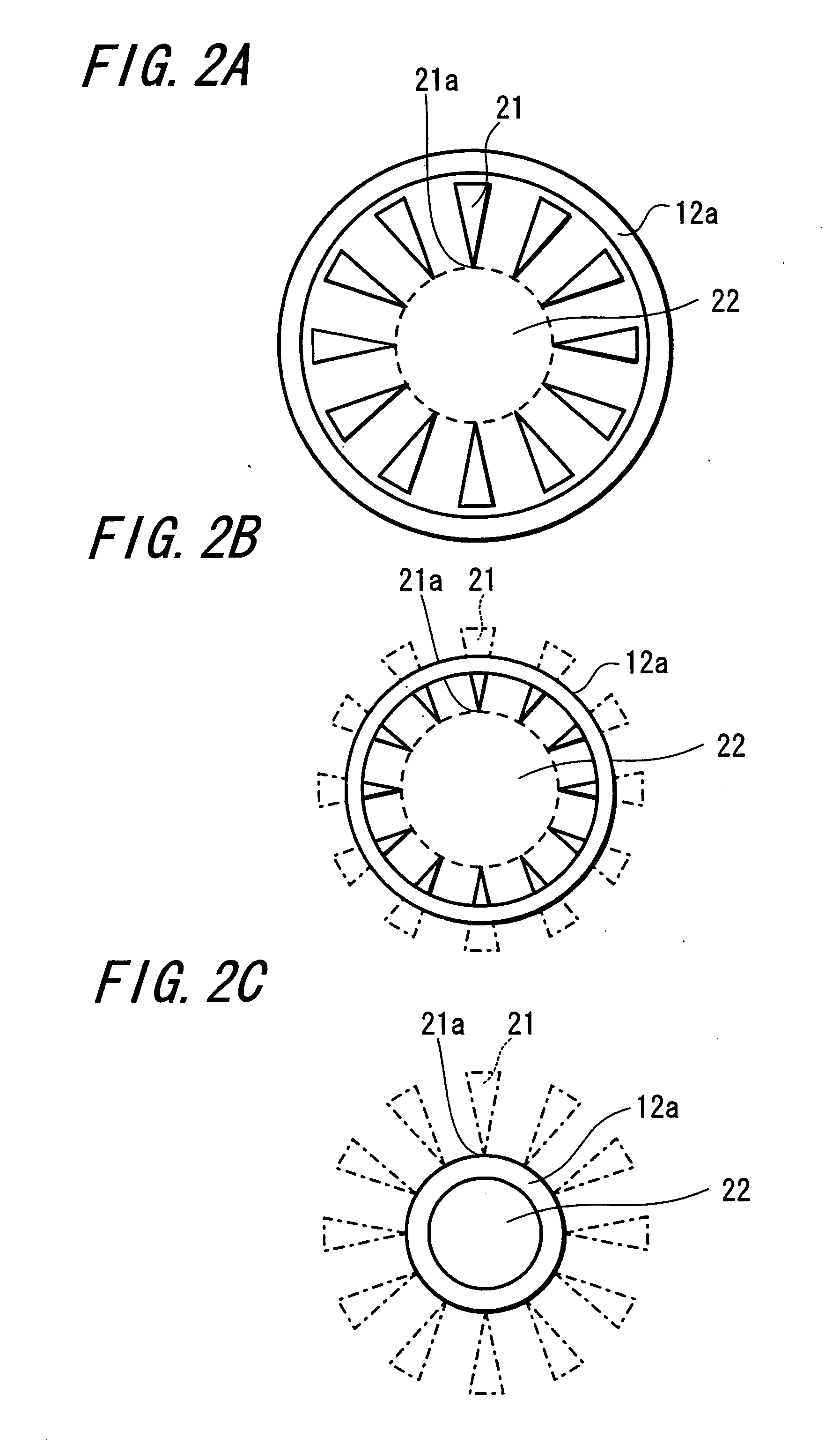
[0062] An example of an embodiment of the surface-emitting semiconductor laser is explained below referring to FIGS. 1 to 4.

[0063]FIG. 1 is a schematic perspective view showing the surface-e...


PUM


Abstract

A surface-emitting semiconductor laser (VCSEL) having a structure in which the single horizontal mode of high power is stably maintained, and an optical device including a light-source device having this surface-emitting semiconductor laser are provided. A scattering-loss-structure portion composed of a low refractive-index region is disposed around a main current path in a surface-emitting semiconductor laser, namely around a cavity structure portion; the low refractive-index region is disposed at intervals; and the shape of the tip portion opposing to the center portion is set to be a tapered shape, for example, at an acute angle. Accordingly, in the cavity structure portion, the loss of light-emitting laser of a high-order mode localized in the outer circumferential portion becomes large, so that a surface-emitting semiconductor laser that oscillates the single-mode laser with favorable performance is constructed.

Description

CROSS REFERENCE TO RELATED APPLICATIONS [0001] This application claims priority to Japanese Patent Application Nos. P2003-367741 filed on Oct. 28, 2003, and P2004-136295 filed on Apr. 30, 2004, the disclosures of which are incorporated by reference herein. BACKGROUND OF THE INVENTION [0002] The present invention relates to a surface-emitting semiconductor laser and a method for manufacturing thereof as well as an optical device including a light-source device in which the surface-emitting semiconductor laser is used. In particular, the present invention relates to a surface-emitting semiconductor laser in which expansion of the mode-field diameter allows for an increase in output with maintaining a single horizontal mode and a method for manufacturing thereof as well as an optical device. [0003] A surface-emitting semiconductor laser is used, for example, as a light-source device for the optical communication when the data communication is performed. [0004] A high power output in su...

Claims


Application Information

Patent Timeline
28 Apr 2005
Publication
US20050089075A1
IPC
H01S5/18; H01S5/183; H01S5/187
CPC
H01S5/18311; H01S5/18316; H01S5/18319; H01S2301/166; H01S5/18391; H01S2301/02; H01S5/18327
Inventors
BABA; MATSUZONO, ATSUSHI