
Infrared transmitter circuit and electronic device

a transmitter circuit and infrared technology, applied in the field of transmitter circuits, can solve the problems of short time in which the device can be used, deterioration or damage of light emission diodes, and increase power consumption, and achieve the effect of reducing power consumption

Inactive Publication Date: 2005-04-28
SHARP KK
View PDF2 Cites 1 Cited by
  • Summary
  • Abstract
  • Description
  • Claims
  • Application Information

AI Technical Summary

Benefits of technology

[0010] The object of the present invention is to provide an infrared transmitter circuit which can reduce power consumption while a protection circuit for stopping supplying a driving current to a light emission diode is operating.
[0012] The infrared transmitter circuit of the present invention includes the protection circuit for preventing the light emission element and the driving circuit from heating and deteriorating. The protection circuit not only stops supplying a driving current to the light emission element but also stops the reference current source, so that a current is hardly consumed by the reference current source. Thus, it is possible to use a battery-driven device provided with the infrared transmitter circuit for a longer period of time.

Problems solved by technology

As a result, the light emission diode is made to excessively emit light, so that the light emission diode is deteriorated or damaged.
As a result, in case where the infrared transmitter circuit is installed on a device, such as a mobile device, which operates on the basis of a battery, a time in which the device can be used is short.
Thus, in a battery-driven device such as a lap top personal computer or a mobile phone provided with the IrDA communication element, the power consumption increases, so that a time in which the device can operate is short.

Method used


Image

  • Infrared transmitter circuit and electronic device
  • Infrared transmitter circuit and electronic device
  • Infrared transmitter circuit and electronic device

Examples


embodiment 1

[Embodiment 1]

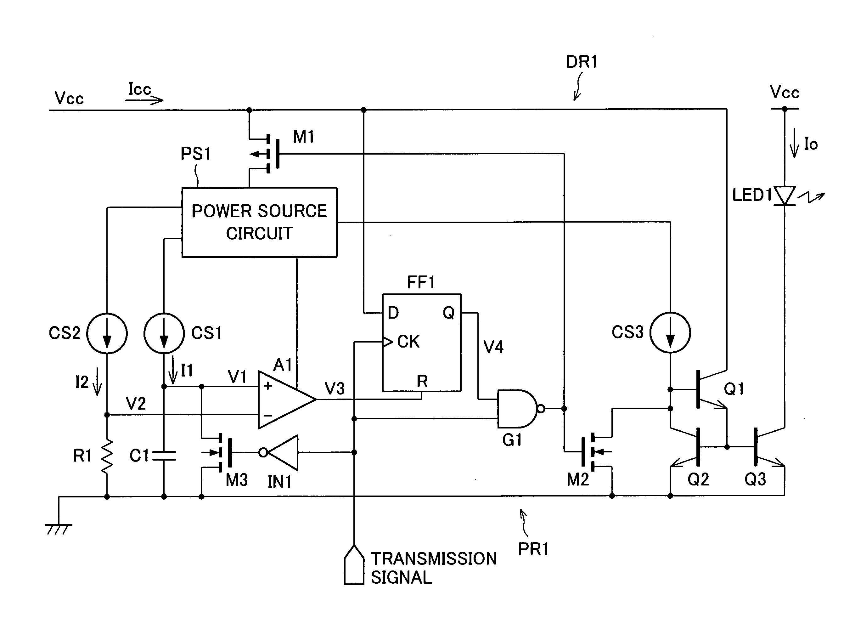
[0031] The following description will explain one embodiment of the present invention with reference to FIG. 1 and FIG. 2.

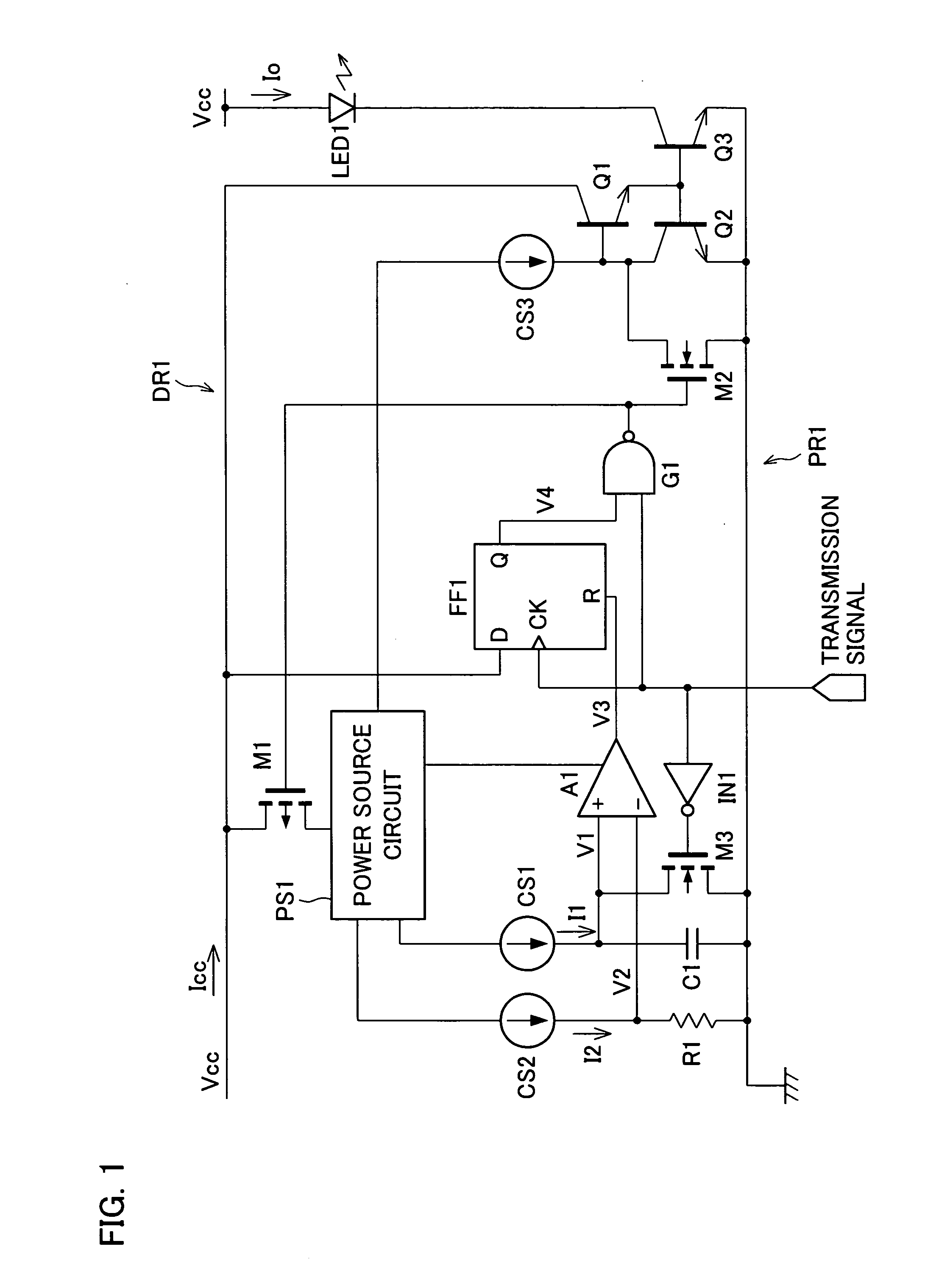
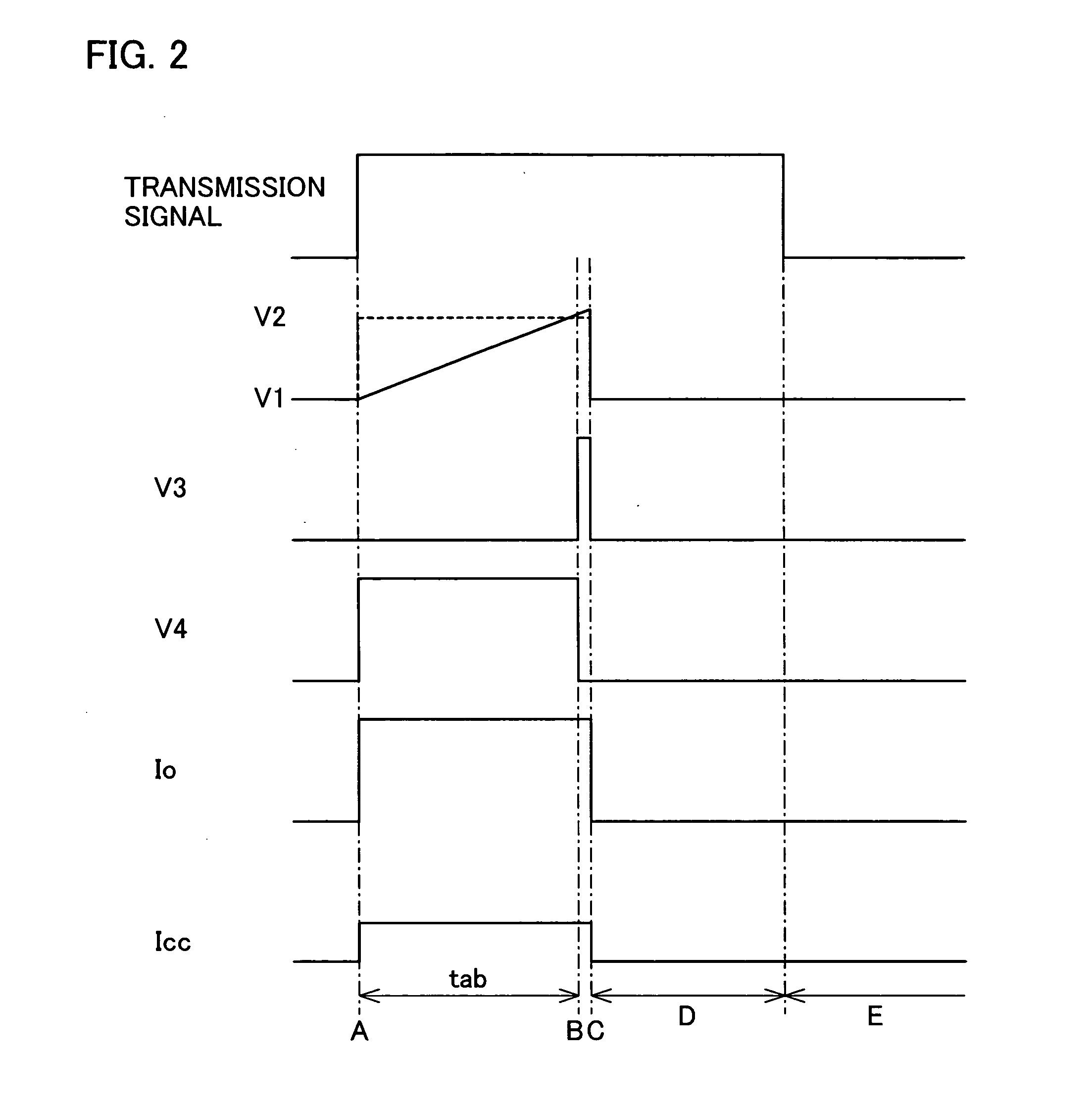
[0032]FIG. 1 shows an arrangement on an infrared transmitter circuit according to the present embodiment. Further, FIG. 2 shows an operation timing of the infrared transmitter circuit.

[0033] As shown in FIG. 1, the infrared transmitter circuit includes a light emission diode LED1 which emits infrared ray as a light emission element. Further, as a driving circuit DR1, the infrared transmitter circuit includes a power source circuit PS1, transistors Q1 to Q3, transistors M1 to M3, constant current sources CS1 to CS3, a NAND gate G1, a D flip-flop FF1, a comparator A1, an inverter circuit IN1, a resistor R1, and a capacitor C1. Each of the infrared transmitter circuit of the present embodiment and infrared transmitter circuits of other embodiments described later is integrated and is provided in an infrared communication element.

[0034] In the infrar...

embodiment 2

[Embodiment 2]

[0052] The following description will explain Embodiment 2 with reference to FIG. 3 to FIG. 5. Note that, in the present embodiment, the same reference signs are given to components having the same functions as those of components described in Embodiment 1, and description thereof is omitted.

[0053]FIG. 3 shows an arrangement of an infrared transmitter circuit according to the present embodiment. Further, FIG. 4 shows an operation timing of the infrared transmitter circuit.

[0054] As shown in FIG. 3, the infrared transmitter circuit is different from the infrared transmitter circuit of Embodiment 1 (FIG. 1) in that: the constant current source CS2, the resistor R1, and the comparator A1 are omitted, and inverter circuits IN2 and IN3 are added. In the infrared transmitter circuit, the transistors M1 to M3, the constant current sources CS1 and CS2, the NAND gate G1, the D flip-flop FF1, the inverter circuits IN1 to IN3, and the capacitor C1 constitute a protection circui...

embodiment 3

[Embodiment 3]

[0076] The following description will explain Embodiment 3 with reference to FIG. 6 and FIG. 7. Note that, in the present embodiment, the same reference signs are given to components having the same functions as those of components described in Embodiments 1 and 2, and description thereof is omitted.

[0077]FIG. 6 shows an arrangement of an infrared transmitter circuit according to the present embodiment. Further, FIG. 7 shows an operation timing of the infrared transmitter circuit.

[0078] As shown in FIG. 6, the infrared transmitter circuit is different from the infrared transmitter circuit of Embodiment 2 (FIG. 3) in that: the constant current source CS1, the inverter circuit IN3, and the D flip-flop FF1 are omitted, and a resistor R2 and a transistor M4 are added. The transistor M4 is a P-channel FET. In the infrared transmitter circuit, the transistors M1 to M4, the NAND gate G1, the inverter circuits IN1 and IN2, the resistor R2, and the capacitor C1 constitute a p...


PUM


Abstract

An infrared transmitter circuit causes an output current to flow to a light emission diode via a current mirror circuit constituted of three transistors by using a current supplied from a power source circuit, so that the light emission diode emits light. When a voltage V1 varied by charging a capacitor with a current flowing from the power source circuit exceeds a reference voltage (voltage V2), an output of a comparator resets a D flip-flop, so that an output of the D flip-flop varies to “0”. Thus, an output of a NAND gate to which that output and a transmission signal are inputted causes a transistor (N-channel FET) to turn ON so as to stop operation of the current mirror circuit, and causes a transistor (P-channel FET) to turn OFF so as to cut a connection between the power source circuit and a power source line. Thus, it is possible to reduce power consumption in operation of a protection circuit which stops supplying the output current to the light emission diode.

Description

[0001] This Nonprovisional application claims priority under 35 U.S.C. § 119(a) on Patent Application No. 2003 / 364938 filed in Japan on Oct. 24, 2003, the entire contents of which are hereby incorporated by reference. FIELD OF THE INVENTION [0002] The present invention relates to a transmitter circuit used to perform infrared communications in which a protection circuit is used to prevent unnecessary lighting of a light emission element. BACKGROUND OF THE INVENTION [0003] Use of a digital signal wireless communication using an infrared ray has been diversified, for example, it is used typically in a remote controller and recently in a mobile device provided with a communication device which is in conformity to an IrDA standard. In the communications, it is general to use an infrared light emission diode to perform data communications. [0004] The infrared light emission diode requires approximately 50 mA as a driving current in sequentially emit light. However, in optical communicati...

Claims


Application Information

Patent Timeline
IPC IPC(8): H03K17/78H04N5/00
CPCH04B10/1141
Inventor ITOH, HIROAKIYOKOGAWA, NARUICHINISHINO, TAKESHIKAWASHIMA, RYOSUKE
Owner SHARP KK
Learn More