Integrated sub-nanometer-scale electron beam systems

a technology of electron beam and sub-nanometer, applied in the direction of electric discharge tube/lamp manufacture, separation process, instruments, etc., can solve the problems of requiring the use of complicated, expensive, cumbersome equipment, etc., and achieves the effect of reducing the number of microscopy probes

Inactive Publication Date: 2005-05-05
BIOMED SOLUTIONS
View PDF30 Cites 116 Cited by
  • Summary
  • Abstract
  • Description
  • Claims
  • Application Information

AI Technical Summary

Problems solved by technology

This often requires the use of complicated, expensive, and cumbersome equipment.
The prior art, however, does not include microscopy probes incorporating superconducting nano-channels comprising carbon-based nanotubes, which are capable of

Method used


Image

  • Integrated sub-nanometer-scale electron beam systems
  • Integrated sub-nanometer-scale electron beam systems
  • Integrated sub-nanometer-scale electron beam systems

Examples


Embodiment Construction

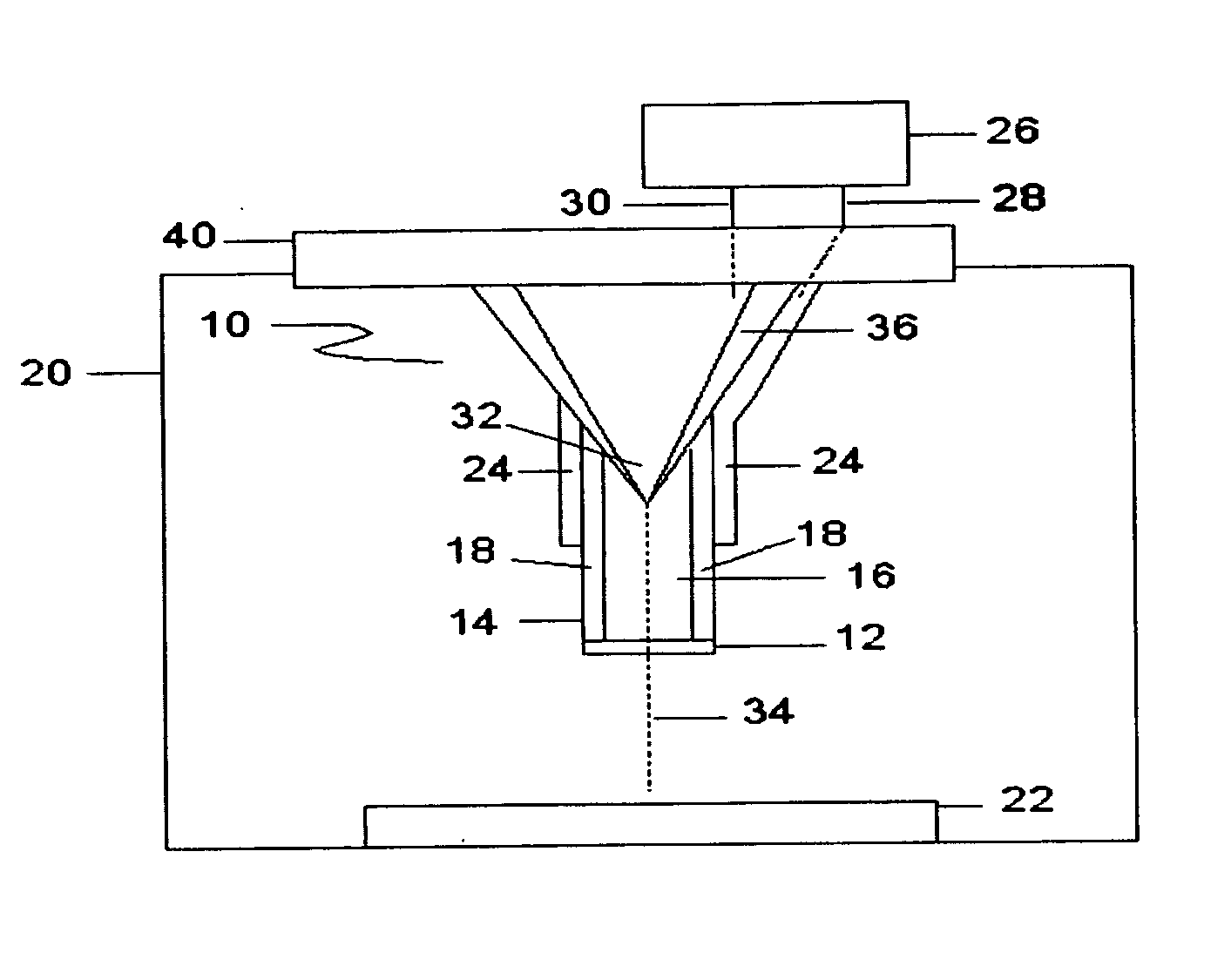
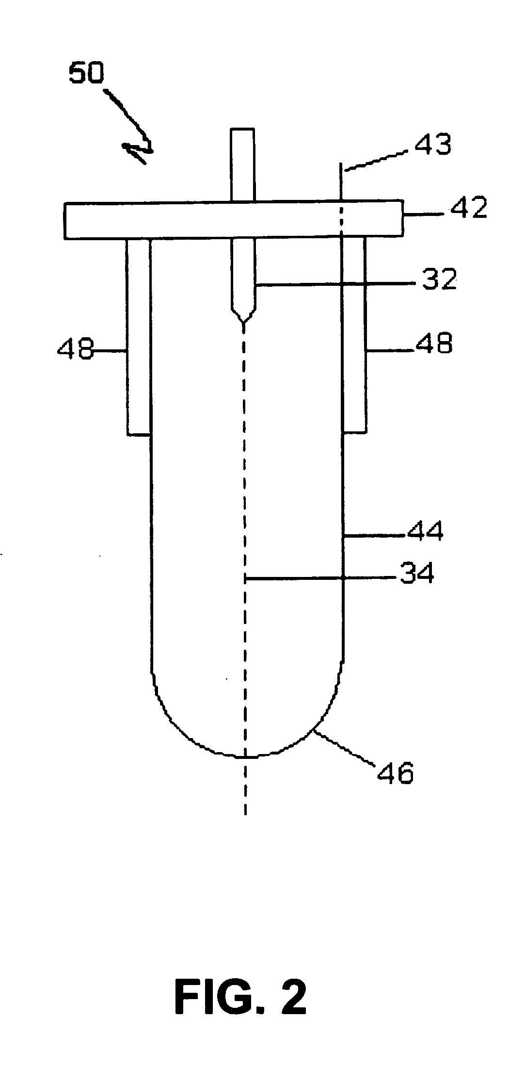
[0068] For a general understanding of the present invention, reference is made to the drawings. In the drawings, like reference numerals have been used throughout to designate identical elements. In describing the present invention, a variety of terms are used in the description. As used herein unless otherwise specified, the term electron beam as used throughout this specification is meant to include any beam comprising charged particles as is known to those skilled in the art.

[0069] Atomic scale point source electron beams have many potential advantages for scanning electron microscopy, including higher resolution at lower voltages in much more compact configurations; these electron beam sources also are advantageously used in vacuum microelectronic devices. The primary disadvantage is the requirement for operation at ultra-high vacuum when used as electron field emitters to avoid damage by ion bombardment. By using a miniature ultra-high vacuum chamber to permanently enclose the...


PUM


Abstract

A solid state sub-nanometer-scale electron beam emitter comprising a multi-layered structure having a nano-tip electron emitter and tunnel emission junction formed on substrate, an initial electron beam extraction electrode, a “nano-sandwich Einzel” electrode, and a topmost protective layer.

Description

CROSS-REFERENCE TO RELATED PATENT APPLICATIONS [0001] This application is a continuation-in-part of co-pending applications, U.S. Ser. No. 10 / 615,452, and U.S. Ser. No. 10 / 615,499, both filed Jul. 8, 2003.[0002] This invention relates generally to highly miniaturized electron beam sources, and particularly to sub-nanometer-scale electron beam sources and systems, fabrication methods thereof, and uses thereof. [0003] As used herein, “sub-nanometer-scale electron beam” designates an electron beams that has most of its energy concentrated in a diameter of approximately one nanometer or less at its point of origin, and possibly also likewise in scale at its principal focal point. Other parts of the beam may be up to 10 times or even 100 times smaller or larger, depending upon the specific application. FIELD OF THE INVENTION [0004] Small-scale electron beam sources, and sub-nanometer-scale electron beam sources, systems, fabrication methods, and uses thereof in particular. BACKGROUND OF ...

Claims


Application Information

Patent Timeline
IPC IPC(8): G21K1/08
CPCG21K1/08G21K5/04H01J1/304H01J3/021H01J9/025H01J37/065H01J2237/1207H01J37/12H01J2201/30407H01J2237/062H01J2237/06341H01J2237/06375H01J2237/1205H01J37/073B33Y80/00
Inventor SCHNEIKER, CONRAD W.
Owner BIOMED SOLUTIONS
Why Eureka
Try Eureka