Semiconductor memory device and method of manufacturing the same

a memory device and semiconductor technology, applied in the direction of semiconductor devices, electrical appliances, transistors, etc., can solve the problems of difficult to improve the manufacturing yield, difficult to achieve good embedding characteristics, and difficult to improve the withstand voltag

Inactive Publication Date: 2005-05-05
KK TOSHIBA
View PDF5 Cites 87 Cited by
  • Summary
  • Abstract
  • Description
  • Claims
  • Application Information

AI Technical Summary

Problems solved by technology

As a result, it becomes difficult to achieve a good embedding characteristic.
Since the conventional semiconductor memory device has the aforementioned structure, and the process of the method of manufacturing the conventional semiconductor memory device is carried out in the manner mentioned above, the following problems have been raised.
Thus, it is difficult to improve the withstand voltage.
Thus, it is difficult to improve the manufacturing yield.
Thus, the aforementioned conventi

Method used


Image

  • Semiconductor memory device and method of manufacturing the same
  • Semiconductor memory device and method of manufacturing the same
  • Semiconductor memory device and method of manufacturing the same

Examples


first embodiment

(First Embodiment)

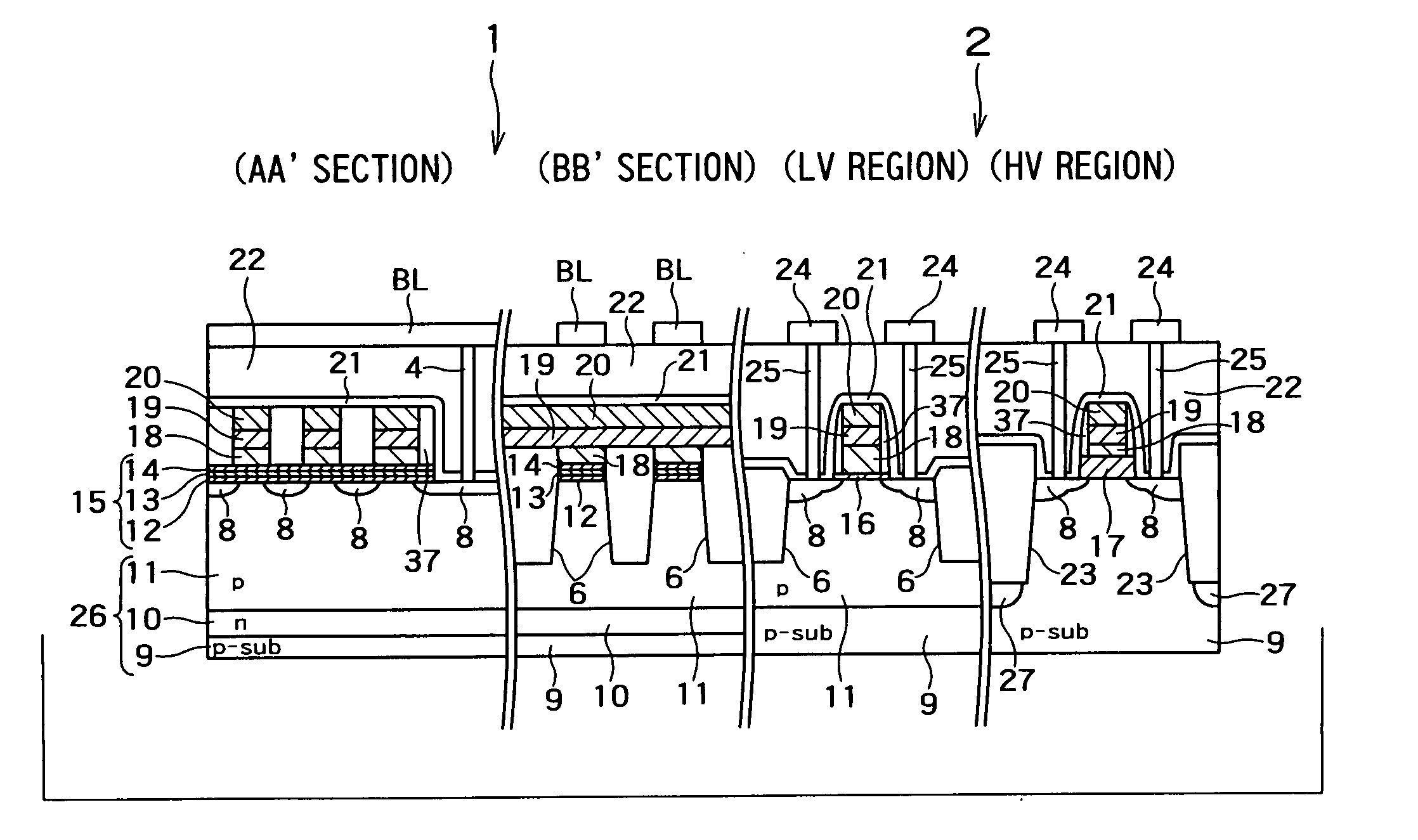
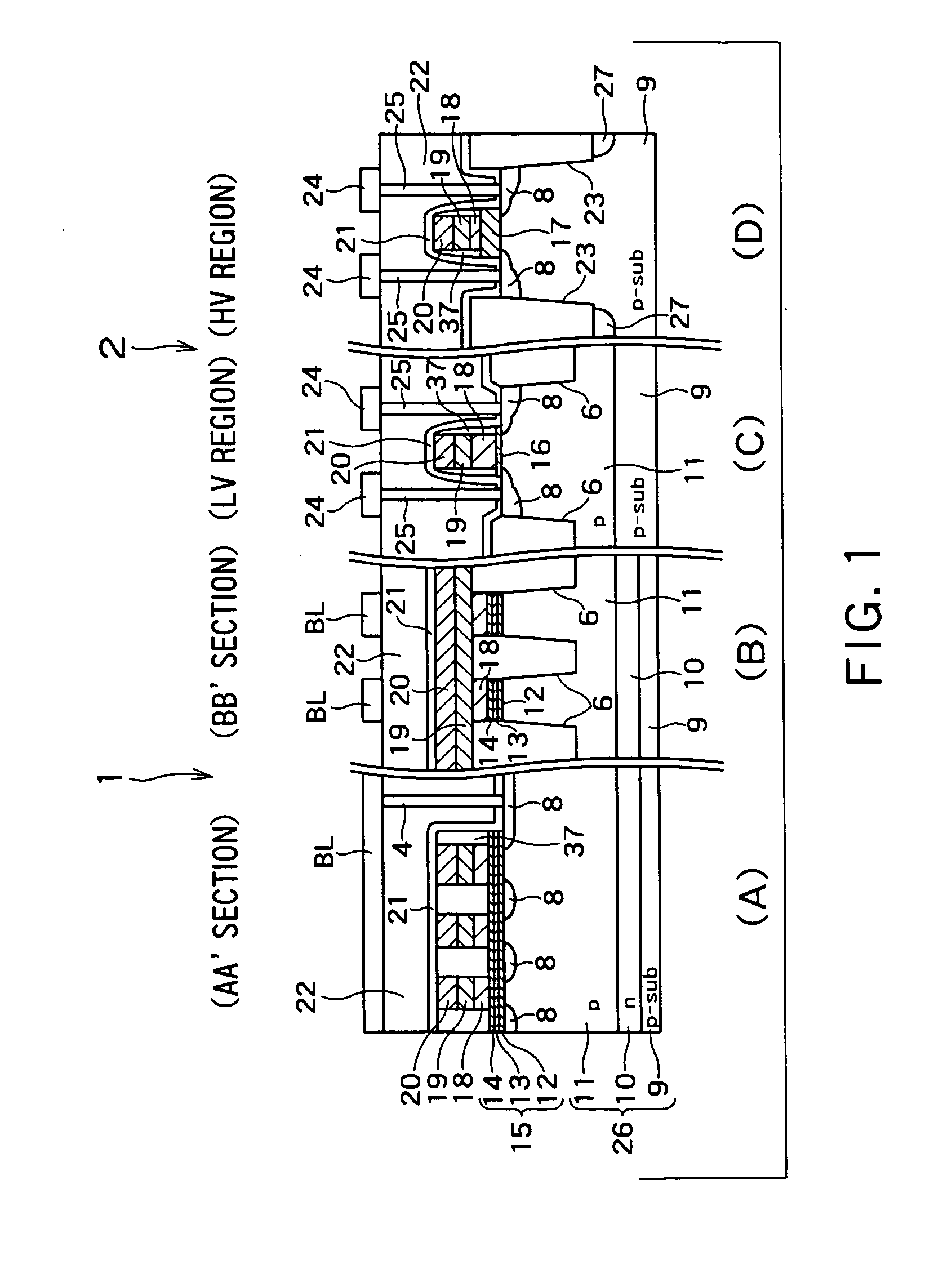
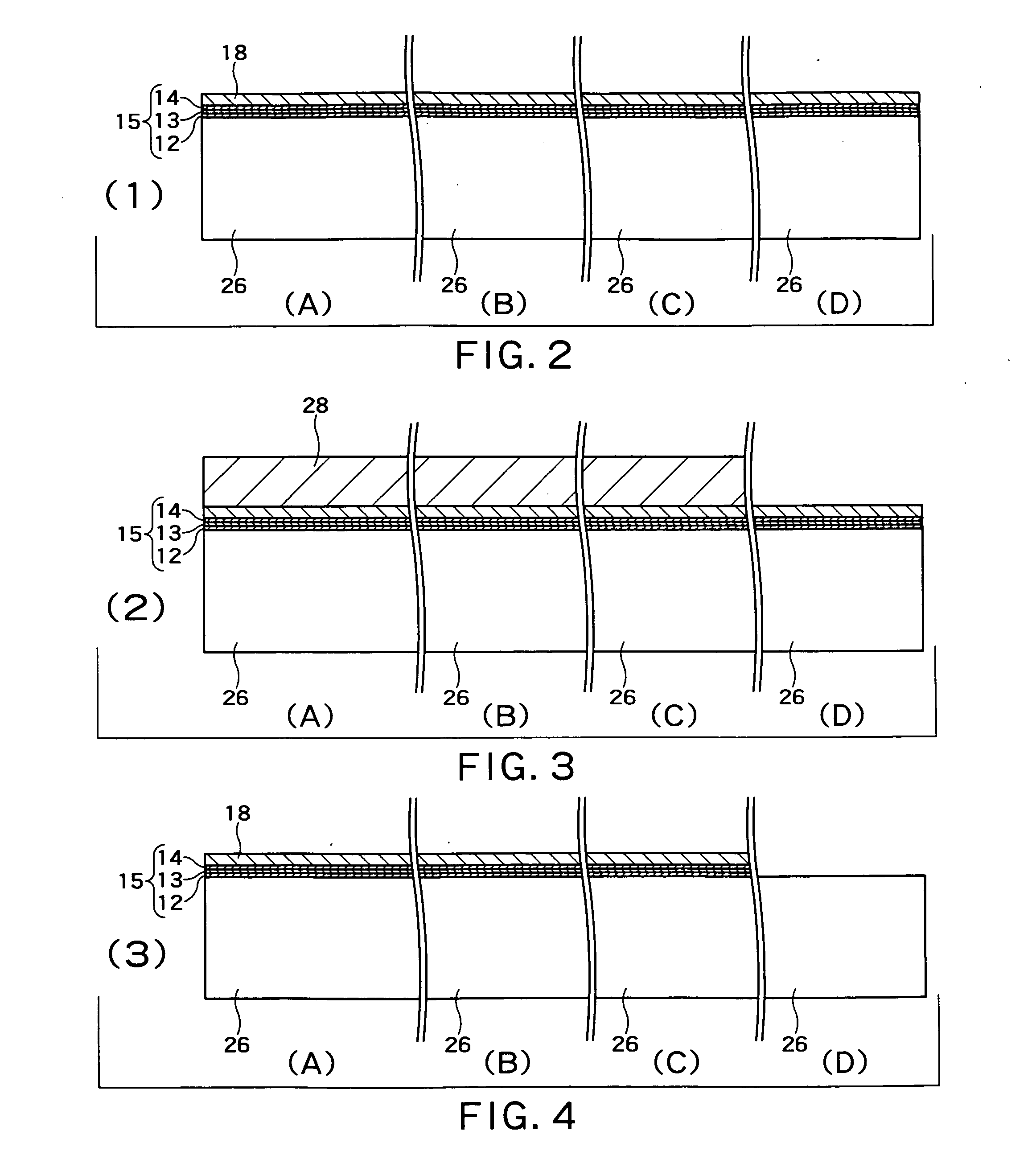
[0137]FIG. 1 shows sectional views of a semiconductor memory device according to a first embodiment of the present invention, in which (A) is a sectional view of a gate of a memory cell region (corresponding to the A-A′ section of FIG. 46), (B) is a sectional view of an element isolation region in the memory cell region (corresponding to the B-B′ section of FIG. 46), (C) is a sectional view of a low voltage transistor region (LV region) of a peripheral circuit portion, and (D) is a sectional view of a high voltage transistor region (HV region).

[0138]FIG. 1 differs from FIG. 47 in that the element isolation groove 23 in the high voltage transistor region of the peripheral circuit portion is deeper than the element isolation grooves 6 in the element isolation region in the memory cell region and the low voltage transistor region in the peripheral circuit portion, as shown in the sections (A), (B), and (C).

[0139] That is, as shown in the sections (B) and (C), in the...

second embodiment

(Second Embodiment)

[0203]FIG. 25 shows sectional views of a semiconductor memory device according to a second embodiment of the present invention, in which (A) shows the gate section in the memory cell region, (B) shows the element isolation section in the memory cell region, (C) shows the low voltage transistor region, and (D) shows the high voltage transistor region.

[0204] The difference between FIGS. 1 and 25 lies in that the gate section in the memory cell region shown in FIG. 25(A).

[0205] In the first embodiment, all of the transistors in the memory cells region, i.e., the transistors for storage, and the transistors for selecting and controlling other transistors, have the same MONOS structure. However, in the second embodiment, the transistors in the memory cell region are divided into two groups, i.e., those located in a storage region 41 for storing information, and those located in a control region 42 for selecting memory cells. The transistors located in the storage reg...

third embodiment

(Third Embodiment)

[0208]FIG. 26 shows sectional views of a semiconductor memory device of the third embodiment. The difference between FIGS. 1 and 26 lies in that the depth of the element isolation grooves 6 in the low voltage transistor region is deeper than the depth of the element isolation grooves 6 in the memory cell region, and substantially the same as the depth of the element isolation grooves 23 in the high voltage transistor region.

[0209] According to the semiconductor memory device of the third embodiment, the element isolation grooves 6 and 23, which should desirably be as deep as possible in order to maintain an element isolation withstand voltage, in the high and low voltage transistor regions are deeper than those in the memory cell region. That is, the semiconductor memory device of this embodiment has a structure suitable for improving withstand voltage.

[0210] In addition, according to the semiconductor memory device of the third embodiment, the element isolation ...


PUM


Abstract

A semiconductor memory device having a memory cell region and a peripheral circuit region, and a method of manufacturing such a semiconductor memory device, are proposed, in which trench grooves are formed to be shallow in the memory cell region in order to improve the yield, and trench grooves are formed to be deep in the high voltage transistor region of the peripheral circuit region, in particular in a high voltage transistor region thereof, in order to improve the element isolation withstand voltage. A plurality of memory cell transistors having an ONO layer 15 serving as a charge accumulating insulating layer are provided in the memory cell region, where element isolation grooves 6 for these memory cell transistors are narrow and shallow. Two types of transistors, one for high voltage and the other for low voltage, having gate insulating layers 16 or 17, which are different from the ONO layer 15 in the memory cell region, are provided in the peripheral circuit region, where at least element isolation grooves 23 for high voltage transistors are wide and deep. In this way, it is possible to improve the degree of integration and yield in the memory cell region, and secure withstand voltage in the peripheral circuit region.

Description

CROSS-REFERENCE TO RELATED APPLICATION [0001] This application is based upon and claims the benefit of priority from prior Japanese Patent Application No. 2003-344689, filed on Oct. 2, 2003, the entire contents of which are incorporated herein by reference. BACKGROUND OF THE INVENTION [0002] 1. Field of the Invention [0003] The present invention relates to a semiconductor memory device and a method of manufacturing the same. In particular, the present invention relates to a semiconductor memory device, in which non-volatile memory cells are highly densely arranged, and highly resistant to a relatively higher voltage, and a method of manufacturing such a semiconductor memory device. [0004] 2. Related Art [0005] So-called MONOS (Metal-silicon Oxide-silicon Nitride-silicon Oxide-Semiconductor) memory cell devices, in which electric charge is trapped into silicon nitride layers, are known as one type of non-volatile semiconductor memory devices capable of being electrically written and ...

Claims


Application Information

Patent Timeline
IPC IPC(8): H01L21/8247H01L21/8246H01L27/00H01L27/105H01L27/108H01L27/115H01L29/788H01L29/792
CPCH01L27/105H01L27/11573H01L27/11568H01L27/115H10B69/00H10B43/30H10B43/40
Inventor GODA, AKIRANOGUCHI, MITSUHIRO
Owner KK TOSHIBA
Why Eureka
Try Eureka