Semiconductor apparatus and method of fabricating the same

a technology of semiconductor devices and semiconductor devices, applied in the direction of electrical devices, semiconductor devices, semiconductor/solid-state device details, etc., can solve problems such as dielectric breakdown between adjacent wirings

Active Publication Date: 2005-05-05
SEMICON COMPONENTS IND LLC
View PDF2 Cites 18 Cited by
  • Summary
  • Abstract
  • Description
  • Claims
  • Application Information

AI Technical Summary

Benefits of technology

[0018] A description of means to achieve the objec

Problems solved by technology

Dielectric breakdown between adjacent wirings mentioned

Method used


Image

  • Semiconductor apparatus and method of fabricating the same
  • Semiconductor apparatus and method of fabricating the same
  • Semiconductor apparatus and method of fabricating the same

Examples


first embodiment

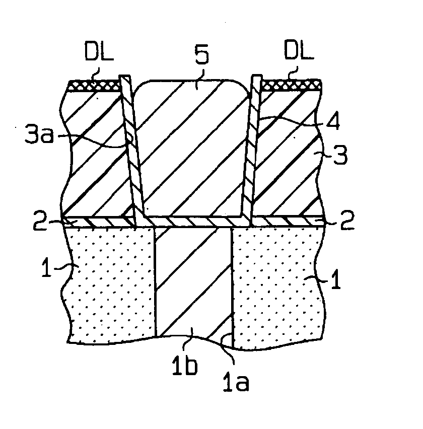
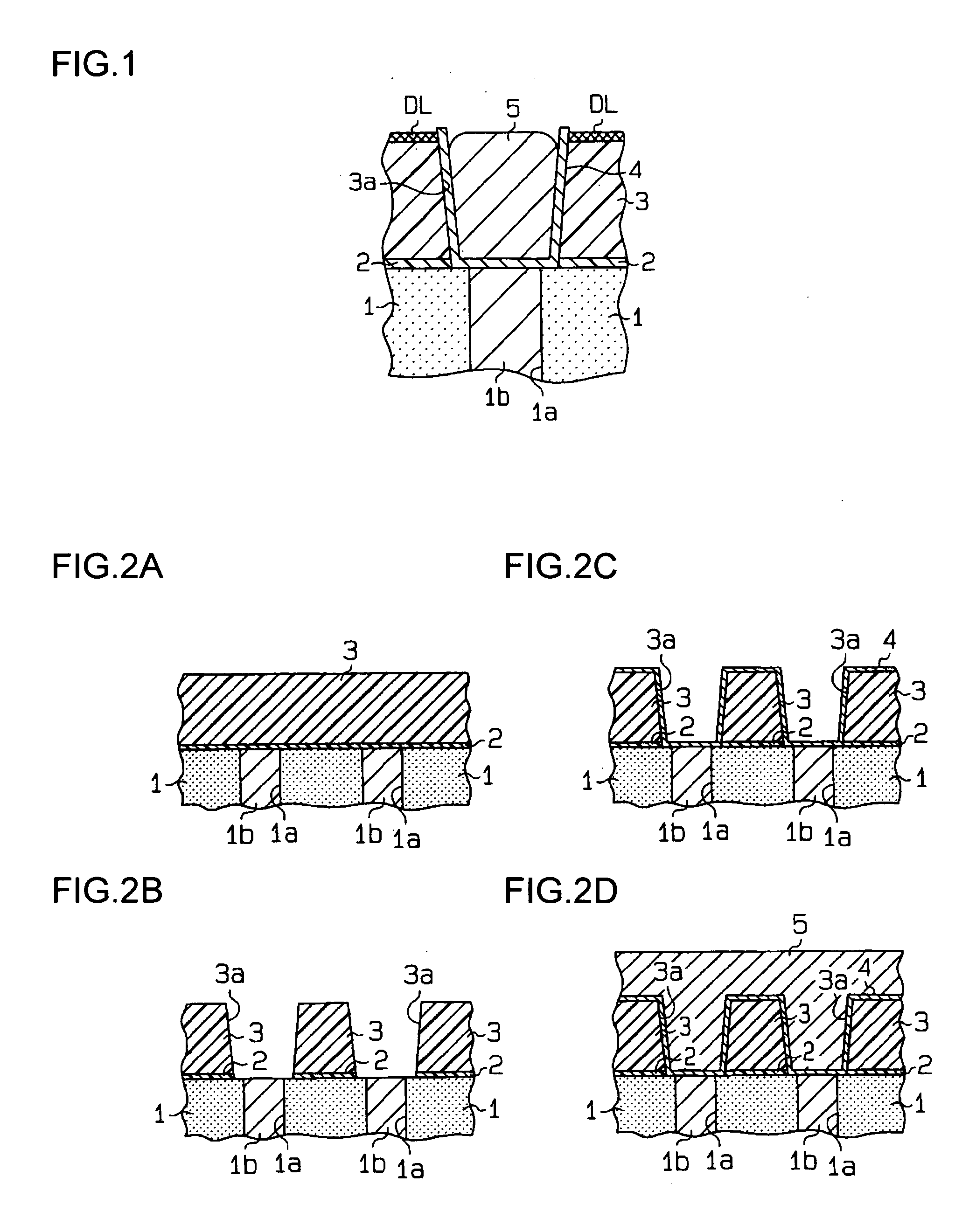
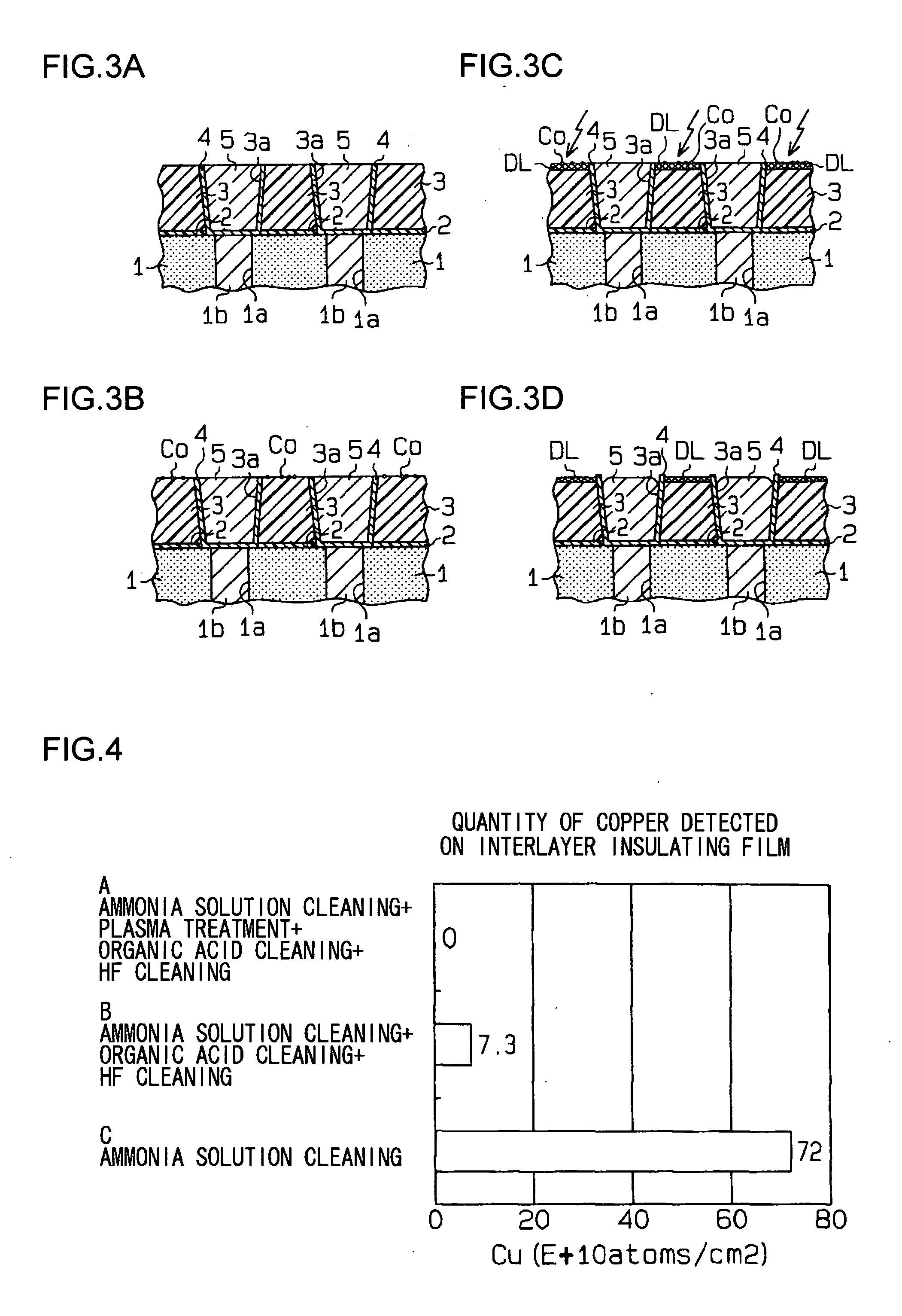
[0074]FIG. 1 shows a semiconductor apparatus according to a first embodiment of the present invention.

[0075] In a similar configuration as the related-art semiconductor apparatus described above, improvement in the TDDB, by suppressing dielectric breakdown occurring between adjacent wirings, is intended as the purpose in the semiconductor apparatus according to the first embodiment. In addition, the semiconductor apparatus according to the embodiment is adapted for suppression of resist poisoning by employing the structure shown in FIG. 1.

[0076] A description will now be given of the structure of the semiconductor apparatus according to the first embodiment by referring to FIG. 1. FIG. 1 shows a schematic section of the semiconductor apparatus according to the first embodiment.

[0077] As shown in FIG. 1, the semiconductor apparatus comprises a stack of: an insulating film 1 formed of silicon oxide or the like; a first interlayer insulating film 2 formed of SiCN or the like capable...

second embodiment

[0112]FIG. 9 shows a semiconductor according to a second embodiment of the present invention.

[0113] In a similar configuration as the semiconductor apparatus shown in FIG. 1, the semiconductor apparatus according to the second embodiment is constructed such that resist poisoning is suppressed and dielectric breakdown between adjacent wirings is suppressed so that the TDDB lifetime is improved. A difference is that the semiconductor apparatus according to the second embodiment has a multilayer wiring structure by building a wiring layer on a substrate in which embedded wiring formed of copper or the like is formed.

[0114] A description will now be given of the structure of the semiconductor apparatus according to the second embodiment, by referring to FIG. 9. FIG. 9 shows a schematic section of the semiconductor apparatus according to the second embodiment.

[0115] As shown in FIG. 9, the semiconductor apparatus comprises a stack of: a substrate 11 in which an embedded wiring formed ...


PUM


Abstract

A semiconductor apparatus is constructed such that the top surface, contacting a barrier metal film, of a conducting film embedded in a trench is located below the top surface of a second interlayer insulating film. The semiconductor apparatus is fabricated such that a plasma treatment is performed in a non-nitriding environment after a polishing process using CMP, so as to form a damaged layer on top of the second interlayer insulating film and the conducting film, and a portion of the damaged layer is removed by etching.

Description

BACKGROUND OF THE INVENTION [0001] 1. Field of the Invention [0002] The present invention generally relates to a semiconductor apparatus and a method of fabricating the same and, more particularly, to a semiconductor apparatus in which a conducting film made of copper is used as a embedded wiring. [0003] 2. Description of the Related Art [0004] It is well known that wiring delay in a semiconductor integrated circuit exercises significant effects as the design rule to fabricate a semiconductor integrated circuit becomes increasingly finer in recent years. The wiring delay is referred to as RC delay. By reducing a product of wiring resistance (R) and wiring capacity (C), the length of delay is controlled. [0005] In the related art exemplified by a patent document No. 1, there is proposed, for control of the delay, a semiconductor apparatus in which copper (Cu), characterized by low resistance than aluminum (Al), is used to form wiring and in which a material of a dielectric constant (...

Claims


Application Information

Patent Timeline
IPC IPC(8): H01L21/306H01L21/768H01L23/52H01L23/532H01L21/3205
CPCH01L21/76807H01L21/76825H01L21/76826H01L21/76829H01L21/76832H01L21/76834H01L21/76877H01L2924/0002H01L21/76883H01L21/76885H01L23/53238H01L2924/00
Inventor NARUSE, YOHKOMATSUBARA, NAOTERUFUJITA, KAZUNORI
Owner SEMICON COMPONENTS IND LLC
Why Eureka
Try Eureka