

Plasma display panel manufacturing method
a technology of plasma display panels and manufacturing methods, applied in the field of plasma display panel manufacturing methods, can solve the problems of reducing the strength of back plates, affecting the appearance of back plates,
- Summary
- Abstract
- Description
- Claims
- Application Information
AI Technical Summary
Problems solved by technology
Method used
Image

Examples
exemplary embodiment 1
[0027] A method of manufacturing PDPs in accordance with the first exemplary embodiment of the present invention is demonstrated hereinafter with reference to the related drawings.
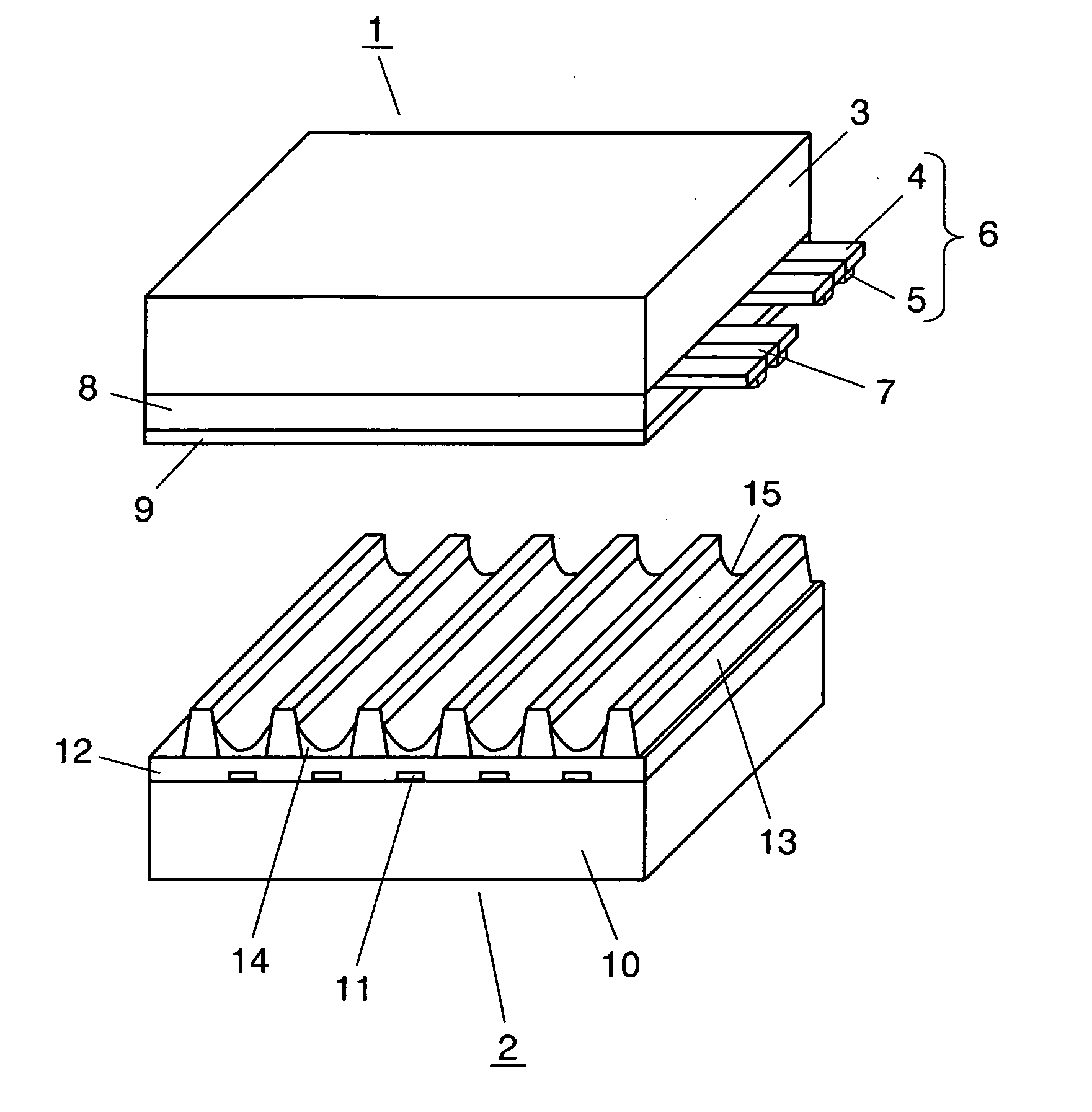
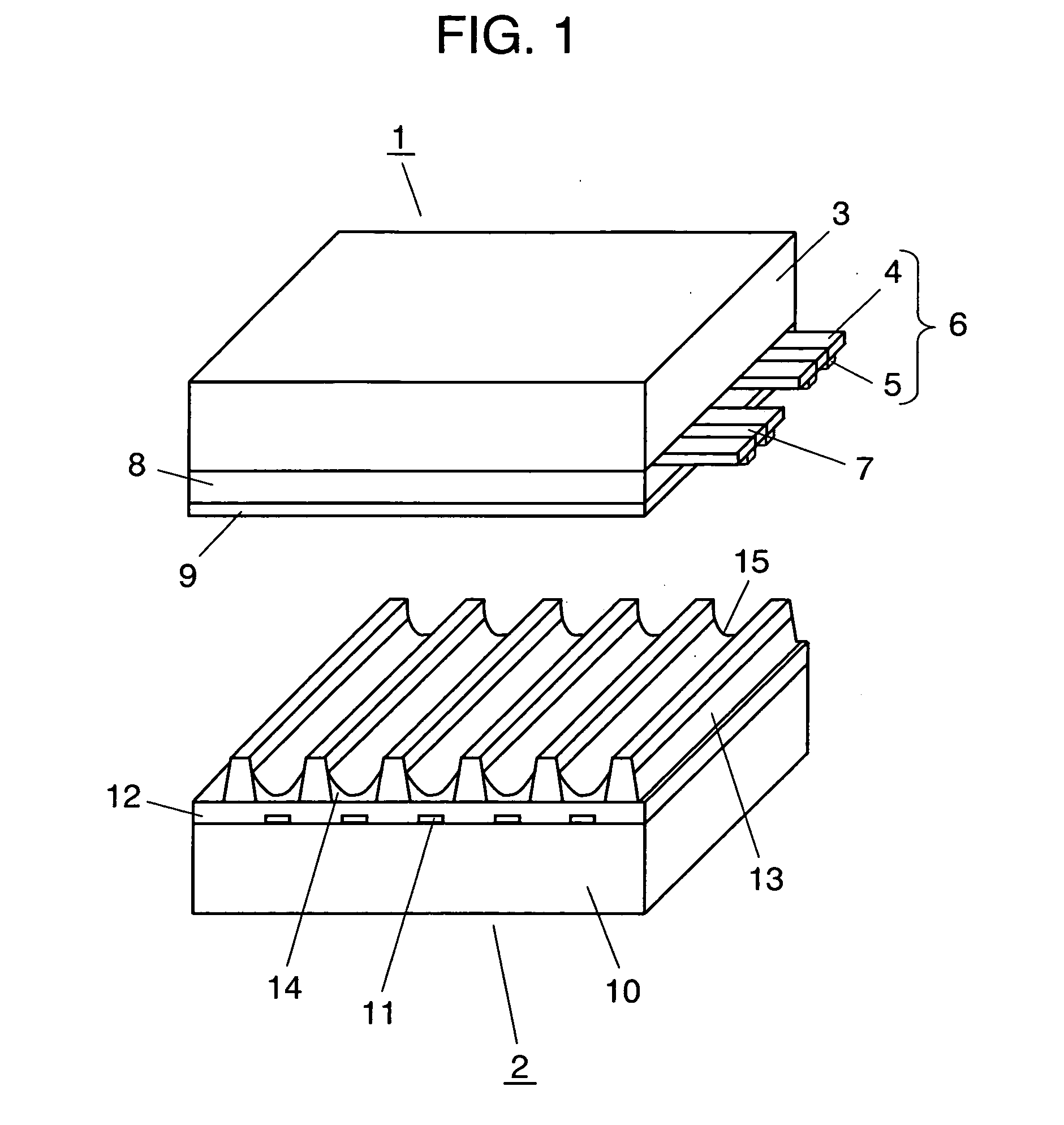
[0028] A structure of the PDP of the present invention is described with reference to FIG. 1. The PDP is basically formed of front plate 1 and back plate 2. Front plate 1 comprises the following elements: [0029] front glass substrate 3; [0030] display electrodes 6 formed on a first principal face of substrate 3 and formed of striped transparent electrodes 4 and bus electrodes 5; [0031] light-proof layers 7 formed on the first principle face of substrate 3; [0032] dielectric layer 8, covering display electrodes 6 and light-proof layers 7, for working as a capacitor; and [0033] protective layer 9 made of magnesium oxide (MgO) and formed on dielectric layer 8. On the other hand, back plate 2 comprises the following elements: [0034] back glass substrate 10; [0035] striped address electrodes 11 formed on a fir...
exemplary embodiment 2
[0055] The second exemplary embodiment of the present invention refers to the case where phosphor layer 14 is equipped with the function of absorbing and collecting the impurity gas.
[0056]FIG. 5 shows a flowchart describing the process of producing phosphor paste by impregnating the degassing material into inorganic material of a phosphor layer as well as the process of forming the phosphor layer using the phosphor paste. In this embodiment, blue phosphor, i.e. BAM:Eu phosphor is used as an example.
[0057] In step 20, the blue phosphor BAM:Eu is prepared, which is compounded in this way: Prepare the following materials in stoichiometrically adequate quantity: aluminum oxide, barium carbonate, and magnesium carbonate as the base material, europium as the activation agent, and a bit of aluminum fluoride as the flux agent that facilitates movement between the materials at partial melting on surface of each material as well as accelerates reactions, then mix the above materials and bak...
exemplary embodiment 3
[0064] The third exemplary embodiment of the present invention refers to a case where back-plate dielectric layer 12 is equipped with the function of absorbing and collecting the impurity gas.
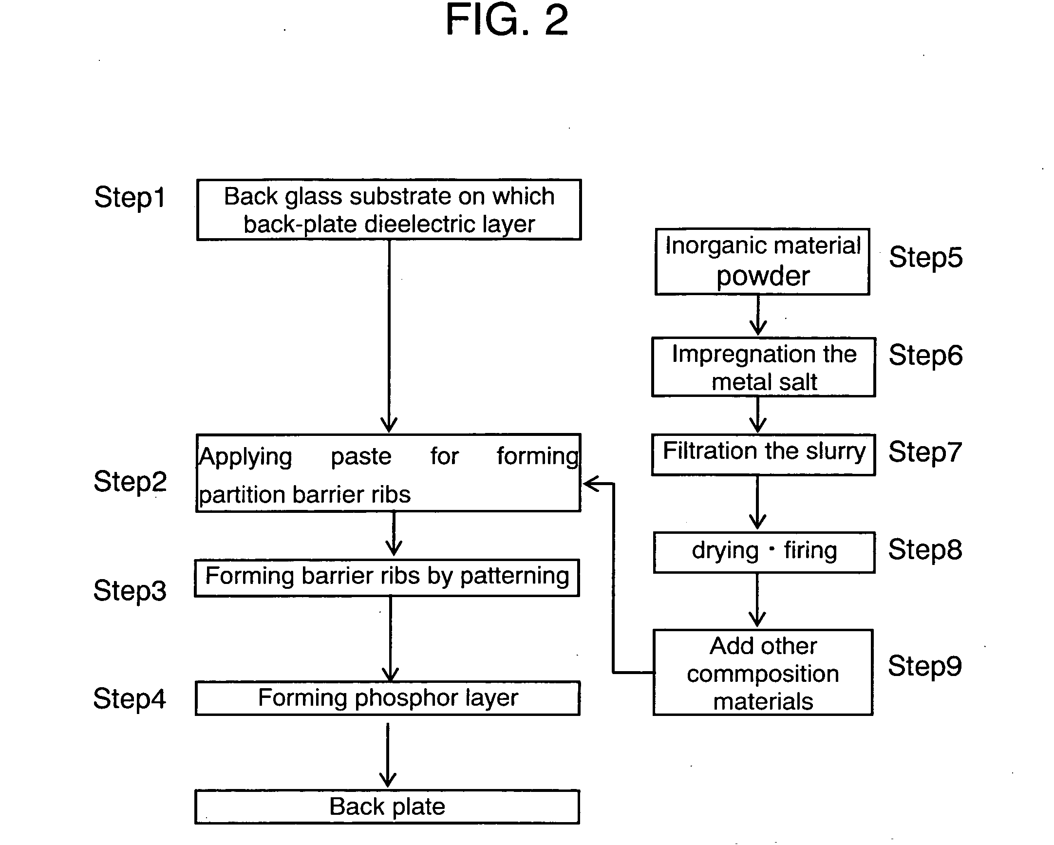
[0065] In step 1 shown in FIG. 2, where a glass substrate having the back-plate dielectric layer is produced, inorganic material of back-plate dielectric layer 12 is impregnated with degassing material for producing dielectric paste. This method is described hereinafter.
[0066] Dielectric layer 8 of front plate 1 needs careful attention to the changes in permeability and dielectric constant depending on the ingredients; however, back-plate dielectric layer 12 does not need such careful attention as layer 8 needs. Thus selection of material, such as inorganic material, e.g. silica or aluminum oxide, impregnated with metal salt of degassing material, can be done with ease. The method of impregnation is similar to the method of impregnation to barrier ribs 13 in accordance with the first embodime...
PUM
 Abstract
Description
Claims
Application Information