Semiconductor device having partially insulated field effect transistor (PiFET) and method of fabricating the same

Active Publication Date: 2005-05-12
SAMSUNG ELECTRONICS CO LTD
View PDF5 Cites 37 Cited by
  • Summary
  • Abstract
  • Description
  • Claims
  • Application Information

AI Technical Summary

Benefits of technology

[0011] Some embodiments of the invention provide methods of fabricating partially insulated field effect transistors (PiFET) that are capable of preventing both short channel effects and floating body effects. Other embodiments of the i

Problems solved by technology

As semiconductor devices become highly integrated, a field effect transistor (FET) using a bulk silicon as a body, as is well known, may experience problems such as short channel effects and an increase in the leakage current.
FETs that

Method used


Image

  • Semiconductor device having partially insulated field effect transistor (PiFET) and method of fabricating the same
  • Semiconductor device having partially insulated field effect transistor (PiFET) and method of fabricating the same
  • Semiconductor device having partially insulated field effect transistor (PiFET) and method of fabricating the same

Examples


Embodiment Construction

[0026] The invention will be described more fully hereinafter with reference to the accompanying drawings, in which several exemplary embodiments of the invention are shown.

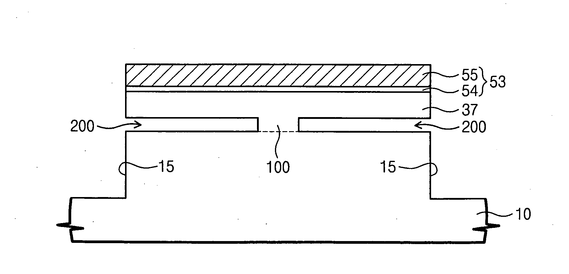
[0027]FIGS. 3A, 4A, 5A, 6A, 7A, and 8A are plan diagrams illustrating a method of fabricating a semiconductor device according to some embodiments of the invention. FIGS. 3B, 4B, 5B, 6B, 7B, and 8B are cross-sectional diagrams taken along the I-I′ lines of FIGS. 3A, 4A, 5A, 6A, 7A, and 8A, respectively. FIGS. 3C, 4C, 5C, 6C, 7C, and 8C are cross-sectional diagrams taken along the II-II′ lines of FIGS. 3A, 4A, 5A, 6A, 7A, and 8A, respectively.

[0028] Referring to FIGS. 3A, 3B, and 3C, a sacrificial layer 20 and a seed semiconductor layer 30 are sequentially formed on a bottom semiconductor layer 10. The seed semiconductor layer 30 and the sacrificial layer 20 are patterned to form at least one opening 99 exposing the bottom semiconductor layer 10 at a predetermined region. At this time, an opening mask pattern 40...


PUM


Abstract

Embodiments of the invention include a partially insulated field effect transistor and a method of fabricating the same. According to some embodiments, a semiconductor substrate is formed by sequentially stacking a bottom semiconductor layer, a sacrificial layer, and a top semiconductor layer. The sacrificial layer may be removed to form a buried gap region between the bottom semiconductor layer and the top semiconductor layer. Then, a transistor may be formed on the semiconductor substrate. The sacrificial layer may be a crystalline semiconductor formed by an epitaxial growth technology.

Description

CROSS REFERENCE TO RELATED APPLICATIONS [0001] This application claims priority from Korean Patent Application No. 2003-0078711, filed on 7 Nov. 2003, the content of which is hereby incorporated by reference in its entirety for all purposes. BACKGROUND OF THE INVENTION [0002] 1. Field of the Invention [0003] This disclosure generally relates to semiconductor devices and methods of fabricating the same. More specifically, this disclosure relates to semiconductor devices having partially insulated field effect transistors and methods of fabricating the same. [0004] 2. Description of the Related Art [0005] As semiconductor devices become highly integrated, a field effect transistor (FET) using a bulk silicon as a body, as is well known, may experience problems such as short channel effects and an increase in the leakage current. FETs that use a substrate having a silicon on insulator (SOI) structure may minimize the above problems but at the cost of increasing the floating body effects...

Claims


Application Information

Patent Timeline
IPC IPC(8): H01L21/336C30B23/00H01L21/331H01L21/762H01L21/8234H01L29/10H01L29/78
CPCH01L21/76283H01L29/78H01L29/1079H01L21/823481H01L21/18
Inventor OH, CHANG-WOOPARK, DONG-GUNCHOE, JEONG-DONGKIM, MIA-SANGKIM, SUNG-MING
Owner SAMSUNG ELECTRONICS CO LTD
Why Eureka
Try Eureka