Multilayer wiring circuit board

a wiring circuit board and multi-layer technology, applied in the direction of thermoplastic polymer dielectrics, dielectric characteristics, semiconductor/solid-state device details, etc., can solve the problems of difficult to make the circuit structure fine, and become impossible to remove high-frequency noise, so as to reduce the inductance of the circuit, suppress the generation of high-frequency noise, and improve the effect of high-frequency switching operation

Inactive Publication Date: 2005-05-12
FUJITSU LTD
View PDF9 Cites 25 Cited by
  • Summary
  • Abstract
  • Description
  • Claims
  • Application Information

AI Technical Summary

Benefits of technology

[0011] Accordingly, it is an object of the present invention to provide an inexpensive multilayer wiring circuit board capable of conducting high frequency switching operation on the circuit while the generation of high frequency noise is being suppressed by reducing the inductance of the circuit.
[0012] It is another object of the present invention to provide a multilayer wiring circuit board on which the generation of high frequency noise, which is generated by an electric power source when switching is conducted on the circuit, is reduced by reducing a distance between the electric power source layer and the mounting parts and also by reducing a distance between the ground electrode and the mounting parts.
[0013] In order to solve the above problems, the present inventors have made investigation in good earnest. As a result of the investigation, the present invention has been accomplished as follows. In order to reduce the generation of high frequency noise by an electronic circuit, a wiring distance between the electric power source and the mounting parts and also a wiring distance between the ground electrode and the mounting parts are minimized so that the circuit inductance between the electric power source and the mounting parts and also between the ground electrode and the mounting parts can be reduced, and further a sectional area of a connection via is optimized. Furthermore, the present inventors have found that the above multilayer wiring circuit board can be produced by the process of producing a conventional printed wiring board.
[0015] According to the present invention, the wiring distances among the electric power source, mounting parts and ground electrode can be minimized, so that it becomes possible to reduce the inductance of the circuit. Therefore, it is possible to provide a multilayer wiring circuit board which does not need a condenser conventionally used for removing high frequency noise generated by the electric power source when switching operation of the circuit is conducted. In this case, the multilayer wiring circuit board can be provided by the same production process as that of a conventional printed wiring board.

Problems solved by technology

Therefore, it is difficult to make the circuit structure fine so as to increase the circuit density by the above conventional method.
When the switching frequency of the circuit is increased more than a predetermined value, it becomes impossible to remove the high frequency noise even if the above conventional circuit structure is adopted.

Method used


Image

  • Multilayer wiring circuit board
  • Multilayer wiring circuit board
  • Multilayer wiring circuit board

Examples


second embodiment

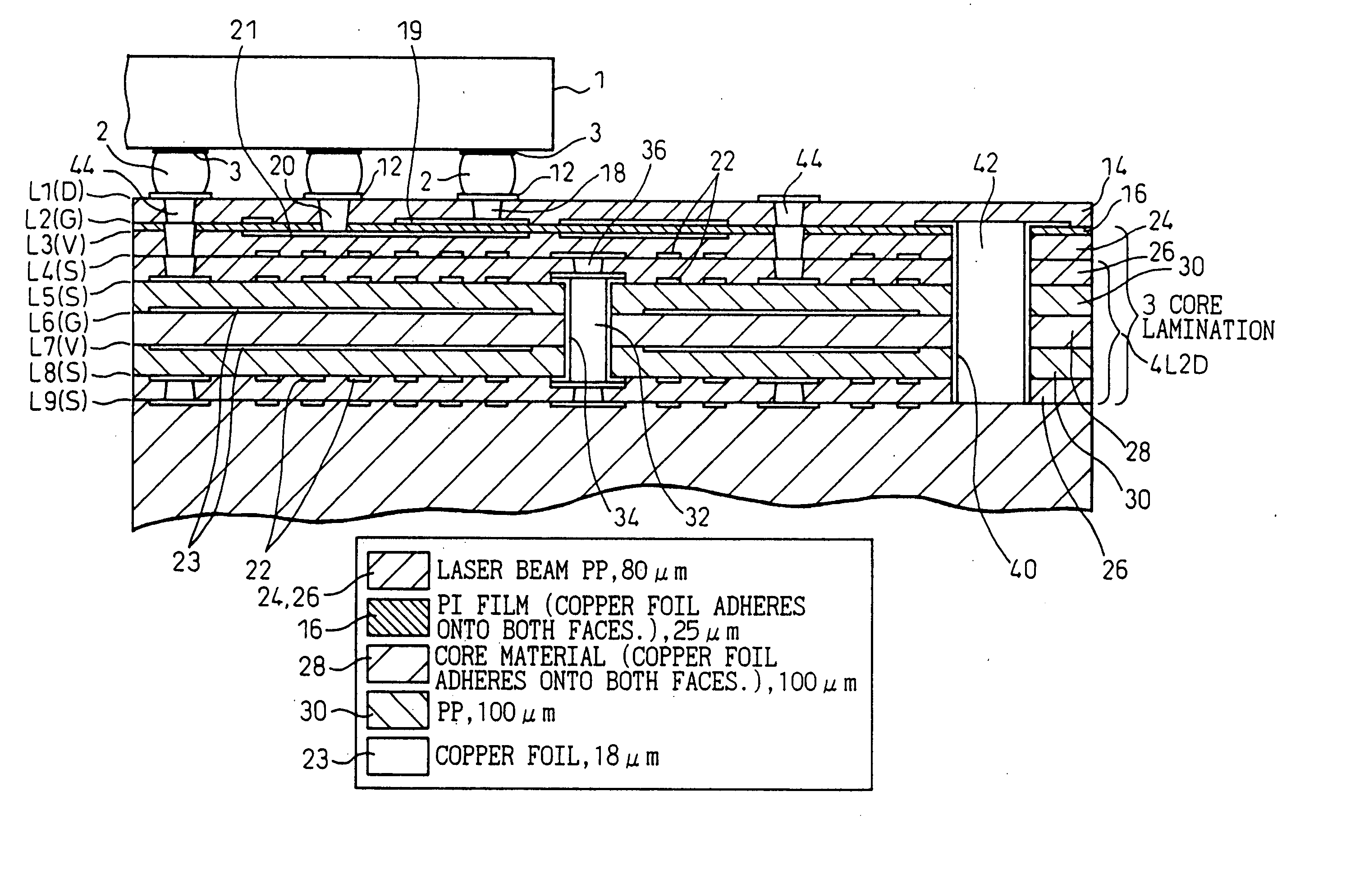
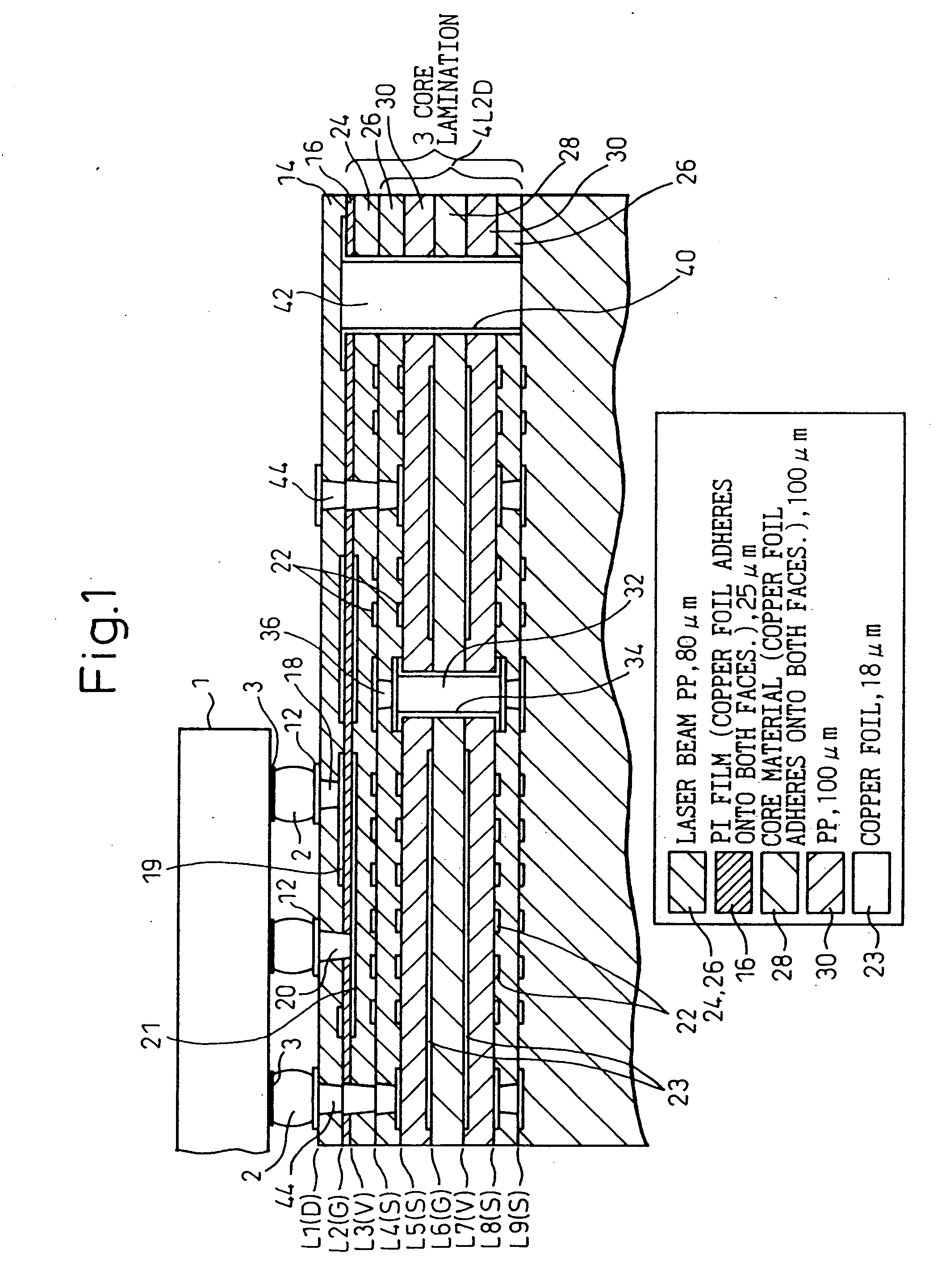
[0101]FIG. 10 is a sectional view of the multilayer wiring circuit board of the present invention.

[0102] In the same manner as that of the first embodiment, concerning the semiconductor chip 1 mounted on the multilayer wiring circuit board of the second embodiment, it is possible to mount any of the bare chip, the ball grid array (BGA) type chip having bumps of the surface mounting type, the LGA type chip having no bumps and the part of QFA type having leads. FIG. 10 is a view showing an example in which the semiconductor chip 1 of the ball grid array (BGA) type having the solder bumps 2 is shown. The electrode pads 3 of this semiconductor chip 1 are connected with pad portions on the conductive pattern 19 provided on the multilayer wiring circuit board via the solder bumps 2.

[0103] The second layer L2 is formed as a ground layer. However, as described later, the conductive pattern connected with the electric power source layer and the signal layer is formed on this second layer. T...

first embodiment

[0104] Between the uppermost surface layer L1 and the ground layer L2, there is provided a surface layer. Instead of the prepreg layer (insulating film) described in the first embodiment, which can be subjected to laser beam patterning, the surface layer is composed of the solder resist layer 14 in this embodiment. The thickness of this solder resist layer 14 is approximately 20 μm. Portions on this solder resist layer 14, in which the solder bumps 2 of the semiconductor chip 1 are joined, are open.

[0105] In the same manner as that of the first embodiment, as the material of the insulating film 16 provided between the ground layer L2 and the electric power source layer L3, it is preferable to use a polyimide film having a thermoplastic adhesion property on both sides. It is possible to use a polyimide film (laser PP) which can be subjected to laser beam patterning, for example, it is possible to use a polyimide film of about 15 μm thickness.

[0106] Concerning the solder resist layer...

third embodiment

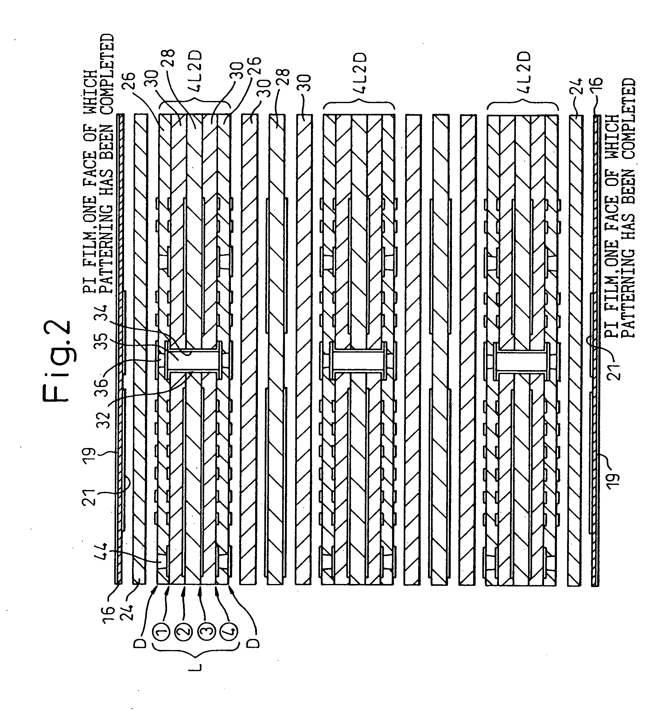
[0118] Accordingly, in the second and the third embodiment, it is unnecessary to provide processes in which the copper foil 48 shown in FIG. 6 is subjected to laser beam machining, plating and patterning.

[0119] In the second and the third embodiment, concerning the copper wiring patterns 19, 21 formed on both faces of the polyimide film 16, one is formed as a ground layer, and the other is formed as an electric power source layer. A portion of the copper wiring pattern 19 on the upper side is connected with the other layer through the conductive vias or copper plating and also connected with the signal layer through the conductive vias or copper plating.

[0120] In any embodiment, both the ground layer and the electric power source layer can be arranged at the closest positions in the thickness direction of the multilayer wiring circuit board compared with the signal layer. Due to the foregoing, it becomes possible to reduce the inductance of the circuit, and the generation of noise ...


PUM

PropertyMeasurementUnit
frequencyaaaaaaaaaa
thicknessaaaaaaaaaa
thicknessaaaaaaaaaa

Abstract

An inexpensive multilayer wiring circuit board capable of conducting high frequency switching operation on the circuit while the generation of high frequency noise is being suppressed by reducing the inductance of the circuit in provided. A multilayer wiring circuit board comprising: an uppermost layer designated as a first layer on which parts are mounted; a second layer on which one of a ground layer and an electric power source layer is arranged; a third layer on which the other is arranged; and an insulating layer arranged between the ground layer and the electric power source layer. A resin layer having a thermoplastic adhesion property on both faces is used as material of the insulating layer arranged between the electric power source layer and the ground layer.

Description

BACKGROUND OF THE INVENTION [0001] 1. Field of the Invention [0002] The present invention relates to a multilayer wiring circuit board used for various electronic equipment and communication equipment. More particularly, the present invention relates to a multilayer wiring circuit board capable of reducing the characteristic impedance in a high frequency region. This invention also relate to a method of producing such a multilayer wiring circuit board. [0003] 2. Description of the Related Art [0004] In order to remove noise, the frequency of which is in a band from 100 to 200 MHz, which is generated by an electric power source when switching is conducted on a circuit, it is conventional that a bypass condenser, which is arranged between the electric power source and the ground, is mounted on a circuit board so that the characteristic impedance can be reduced by increasing the capacitance of the circuit. [0005] However, according to the above method by which the characteristic impeda...

Claims


Application Information

Patent Timeline
Patent Type & Authority Applications(United States)
IPC IPC(8): H05K1/11H05K3/00H05K3/46H05K1/02
CPCH01L2224/16225H01L2924/01087H05K1/113H05K3/0035H05K3/4602H05K3/4623H05K3/4626H05K3/4641H05K3/4652H05K3/4655H05K3/4688H05K2201/0129H05K2201/0154H05K2201/09309H05K2201/09518H05K2201/09536H05K2201/096H05K2203/1394H05K1/0216H01L2224/05573H01L2224/05568
Inventor KUSAGAYA, TOSHIHIROYONEDA, YASUHIROMIZUTANI, DAISUKEIIJIMA, KAZUHIKOSUWA, YUJI
Owner FUJITSU LTD
Why Eureka
Try Eureka