Method for fabricating array substrate of liquid crystal display device

Active Publication Date: 2005-05-12
LG DISPLAY CO LTD
View PDF2 Cites 24 Cited by
  • Summary
  • Abstract
  • Description
  • Claims
  • Application Information

AI Technical Summary

Benefits of technology

[0020] An object of the present invention is to provide an array substrate of a liquid crystal display (LCD) device and a method for fabricating the same in order to decrease the unit cost and time of fabrication by decreasing the number of masks used.
[0023] The array substrate of the LCD device according to the present invention requires 3 masks, whereby it is possible to decrease the fabrication cost and time by decreasing the number of masks used.

Problems solved by technology

The method for fabricating the array substrate of the LCD device according to the related art requires 5 masks when forming the gate line layer, semiconductor layer, the data line layer, the contact hole of the passivation layer and the pixel electrode, thereby lowering fabrication efficiency due to the complicated fabrication process and the increase of fabrication time and cost.

Method used


Image

  • Method for fabricating array substrate of liquid crystal display device
  • Method for fabricating array substrate of liquid crystal display device
  • Method for fabricating array substrate of liquid crystal display device

Examples


Embodiment Construction

[0030] Reference will now be made in detail to the preferred embodiments of the present invention, examples of which are illustrated in the accompanying drawings. Wherever possible, the same reference numbers will be used throughout the drawings to refer to the same or like parts.

[0031] Hereinafter, an array substrate of an LCD device according to the present invention and a method for fabricating the same will be described with reference to the accompanying drawings.

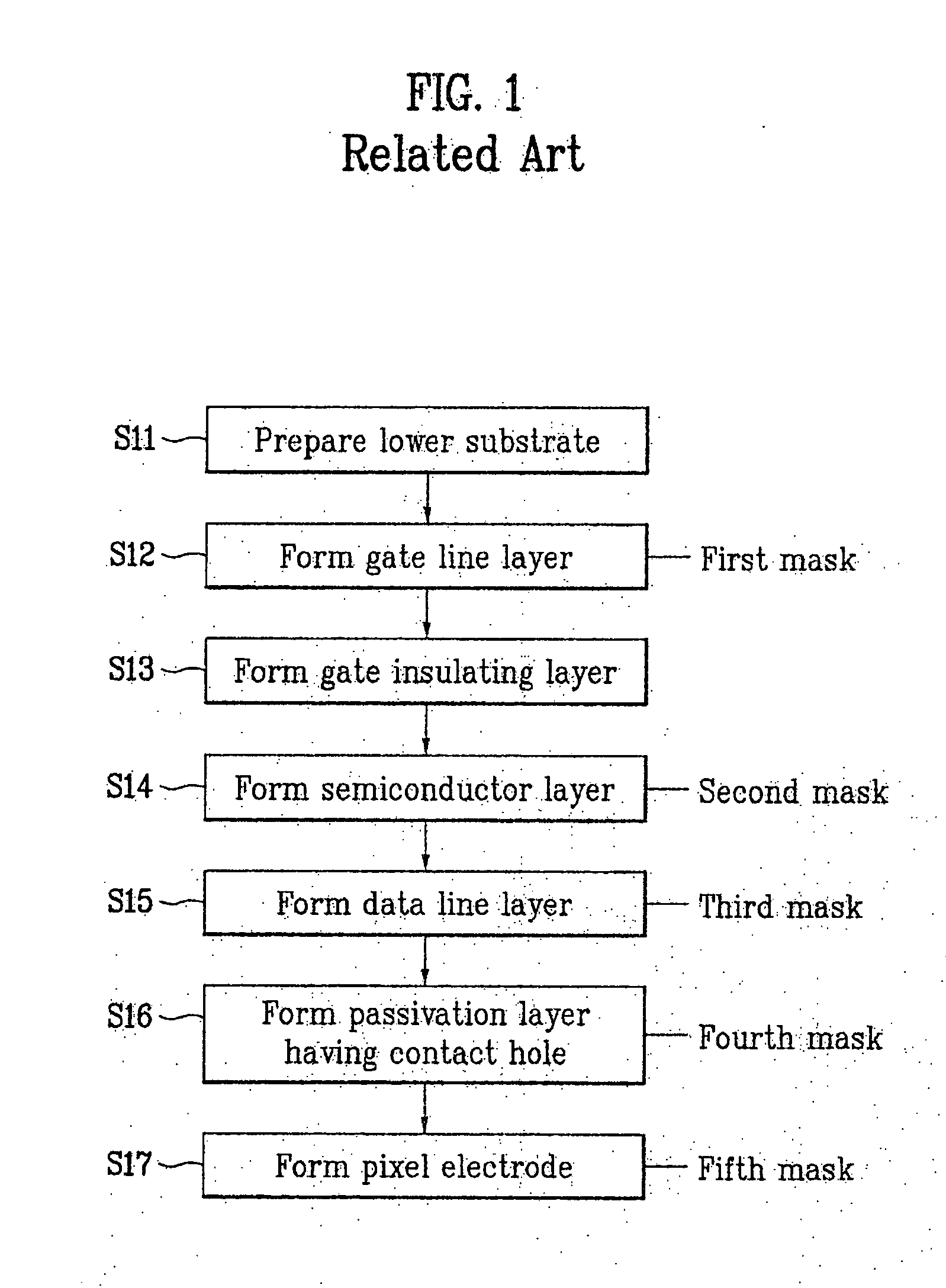
[0032]FIG. 3 is a flow chart illustrating the fabrication process of an array substrate according to the present invention. FIG. 4A to FIG. 4H are plan and cross-sectional views illustrating the fabrication process of an array substrate according to the present invention.

[0033] To form the array substrate of the LCD device according to the present invention, as shown in FIG. 3, a transparent conductive layer and a low-resistance metal layer are deposited on a prepared substrate, and a gate line layer and a pixel elec...


PUM


Abstract

An array substrate of a liquid crystal display (LCD) device and a method for fabricating the same is disclosed, to decrease the unit cost and time of fabrication by decreasing the usage count of mask, which includes simultaneously forming a gate line, a gate electrode and a pixel electrode on a substrate; depositing a gate insulating layer and an active layer on an entire surface of the substrate including the gate line; patterning the gate insulating layer and the active layer to remain on the gate line and the gate electrode; selectively removing the active layer above the gate line; forming a data line perpendicular to the gate line and source / drain electrodes; and depositing a passivation layer on the entire surface of the substrate including the data line.

Description

[0001] This application claims the benefit of Korean Patent Application No. P2003-75508, filed on Oct. 28, 2003, which is hereby incorporated by reference for all purposes as if fully set forth herein. BACKGROUND OF THE INVENTION [0002] 1. Field of the Invention [0003] The present invention relates to a liquid crystal display (LCD) device, and more particularly, to a method for fabricating an array substrate of an LCD device, to decrease the number of masks used. [0004] 2. Discussion of the Related Art [0005] Liquid crystal display (LCD) devices have been widely used due to the advantageous characteristics of high contrast ratio, improved gray and image display and low power consumption. To operate the LCD device, it is necessary to form various patterns of driving devices or lines on a substrate of the LCD device, wherein photolithography is generally used to form patterns on the substrate. To form the patterns on the substrate by photolithography, a photoresist coats the substrate...

Claims


Application Information

Patent Timeline
IPC IPC(8): H01L21/00H01L21/77G02F1/136H01L21/84H01L27/12
CPCH01L27/1288H01L27/1214H01L27/124G02F1/136
Inventor CHO, HEUNG LYULNAM, SEUNG HEEOH, JAE YOUNG
Owner LG DISPLAY CO LTD
Why Eureka
Try Eureka