Method and system for hermetically sealing packages for optics

a technology of optics and packaging, applied in the field of manufacturing objects, can solve the problems of unsuitable packages for many mems applications, unsuitable packages for this application, and non-uniform index of refraction

Active Publication Date: 2005-05-12
MIRADIA INC
View PDF19 Cites 76 Cited by
  • Summary
  • Abstract
  • Description
  • Claims
  • Application Information

AI Technical Summary

Problems solved by technology

The package illustrated in FIG. 1 presents several drawbacks in applications that often require more than electrical operation of the silicon integrated circuit.
The optical properties of the plastic encapsulant, including lack of transparency, non-uniformity of the index of refraction, and surface roughness make these packages unsuitable for this application.
The physical contact that the plastic encapsulant makes with the surface of the integrated circuit, therefore, make this package unsuitable for many MEMS applications.

Method used


Image

  • Method and system for hermetically sealing packages for optics
  • Method and system for hermetically sealing packages for optics
  • Method and system for hermetically sealing packages for optics

Examples


Embodiment Construction

[0017] According to the present invention, techniques for manufacturing objects are provided. More particularly, the invention provides a method and system for hermetically sealing packages for objects. Merely by way of example, the invention has been applied to the hermetic sealing of an optical micro-mirror package. The method and system can be applied to sensor technology as well as other MEMS devices where hermetic packaging is required.

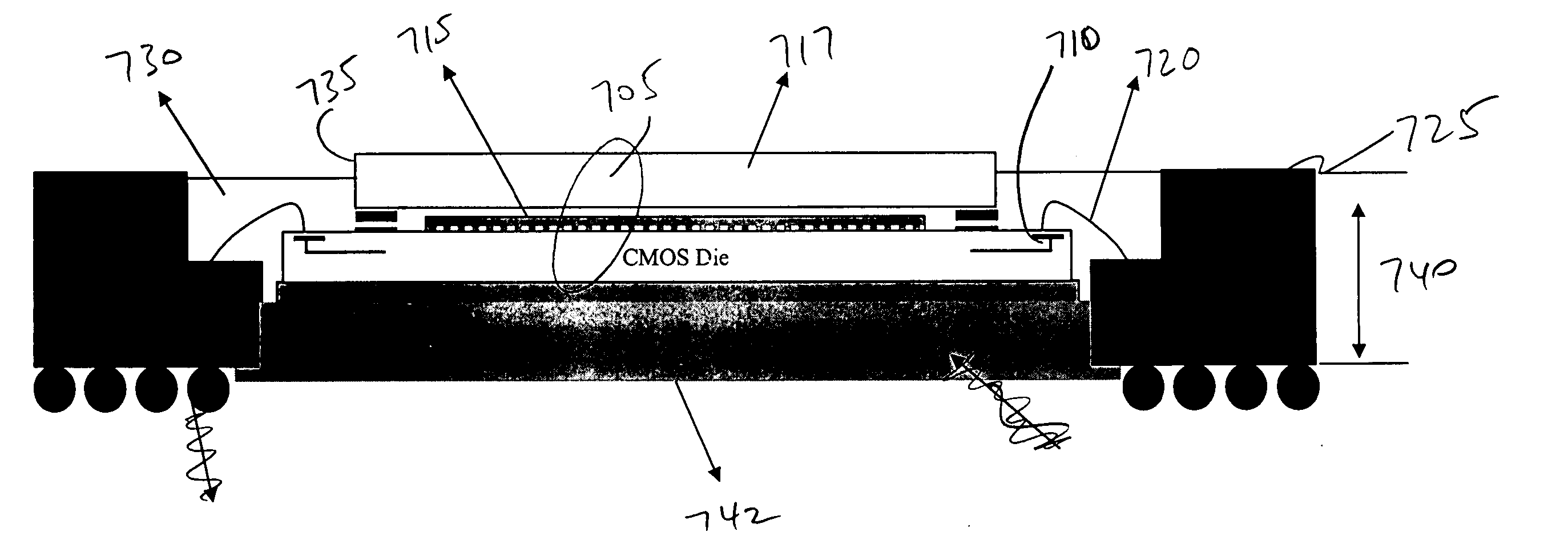
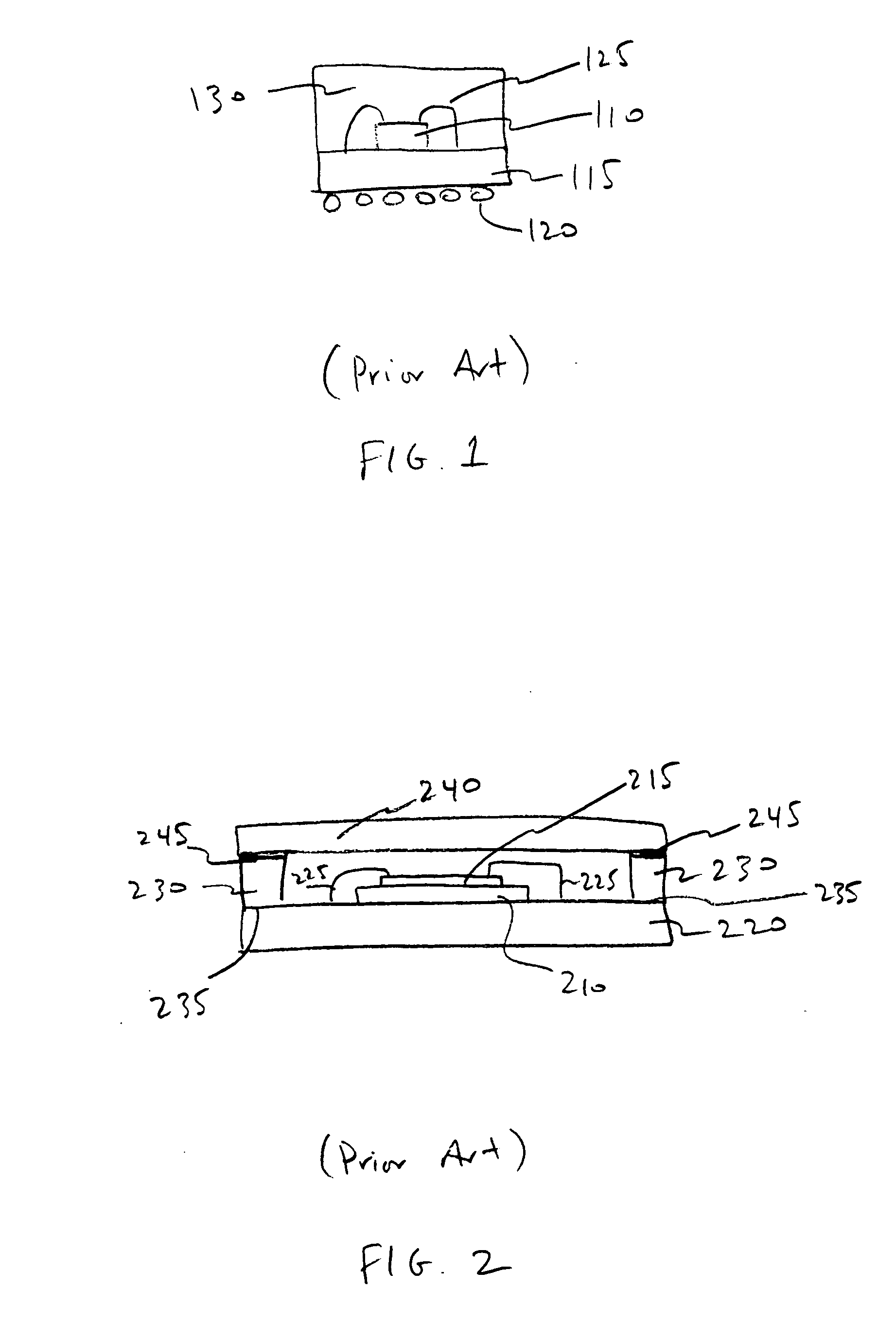
[0018]FIG. 2 illustrates a simplified diagram of a conventional hermetically sealed transparent integrated circuit package useful for optical illumination of a micro-mirror array. In FIG. 2, a silicon MEMS die 210 featuring a micro-mirror array 215 is mounted on a submount 220. The die is attached to the submount using die attach procedures that are compatible with hermetically sealed packaging requirements well known to those skilled in the art. Wire bonds 225 are attached to the silicon die and the submount as with the package illustrated in F...


PUM

PropertyMeasurementUnit
widthaaaaaaaaaa
optical power transmittanceaaaaaaaaaa
thicknessaaaaaaaaaa

Abstract

A method for hermetically sealing devices. The method includes providing a substrate which includes a plurality of individual chips. Each of the chips includes a plurality of devices and each of the chips are arranged in a spatial manner as a first array. The method also provides a transparent member of a predetermined thickness which includes a plurality of recessed regions arranged in a spatial manner as a second array and a standoff region. The method also includes aligning the transparent member in a manner to couple each of the plurality of recessed regions to a respective one of said plurality of chips. The method further includes hermetically sealing each of the chips within one of the respective recessed regions by using at least a bonding process to isolate each of the chips within one of the recessed regions.

Description

BACKGROUND OF THE INVENTION [0001] This present invention relates generally to manufacturing objects. More particularly, the invention provides a method and structure for hermetically bonding a transparent cover to a semiconductor substrate. Merely by way of example, the invention has been applied to a transparent glass cover hermetically bonded to a semiconductor wafer containing a micro-mechanical electrical system. The method and structure can be applied to display technology as well as, for example, charge coupled display camera arrays, and infrared arrays. [0002] The packaging of silicon integrated circuits has reached a high level of maturity. FIG. 1 illustrates a simplified diagram of a conventional silicon integrated circuit package. The silicon integrated circuit die 110 is mounted on a submount 115 featuring a ball grid array 120. Wire bonds 125 are attached to the silicon die 110 to provide electrical connection to the submount 115. Typically, the silicon die 110 and the ...

Claims


Application Information

Patent Timeline
Patent Type & Authority Applications(United States)
IPC IPC(8): H01L23/10G02B6/42G02B26/08H01L21/50H01L23/02H01L23/08H01L27/14H01L31/0203
CPCG02B26/0833Y10T156/1092H01L27/14618H01L27/14621H01L31/0203H01L2224/48091H01L2224/48227H01L2924/01079H01L2924/15311H01L21/50Y10T156/1093H01L2924/1461H01L2924/3025H01L2924/10253H01L2224/45144H01L2924/01322H01L2924/01021H01L2924/00014H01L2924/00H01L2924/16195H01L2924/181H01L2924/00012H01L23/02H01L23/08H01L27/14
Inventor YANG, XIAO
Owner MIRADIA INC
Why Eureka
Try Eureka