Method of forming metal line in semiconductor device

a metal line and semiconductor technology, applied in semiconductor devices, semiconductor/solid-state device details, electrical devices, etc., can solve the problems of reducing excessive removal of insulation film, and inability to obtain metal line insulation film, so as to prevent the reliability of the metal line from being reduced, and high integration tendency of the semiconductor devi

Inactive Publication Date: 2005-05-12
MICRON TECH INC
View PDF3 Cites 6 Cited by
  • Summary
  • Abstract
  • Description
  • Claims
  • Application Information

AI Technical Summary

Benefits of technology

[0006] The present invention is directed to a method for forming a metal line in a semiconductor device which can prevent reliability of the metal line from being reduced due to a high integration tendency of the semiconductor device.
[0008] Preferably, the step for removing the second insulation film reduces a width and thickness of the trenches as well as a thickness of the etch barrier film.

Problems solved by technology

Recently, an insulation film for a metal line is not easily obtained due to a high integration tendency of a semiconductor device, and thus a process for forming a metal line by using a damascene process increasingly generates a short between the metal lines, namely a crosstalk.
However, the insulation film is excessively removed due to general processes such as a photoetching process, a cleaning process performed before filling a metal material, and a plariarization process performed after filling the metal material, and thus has a smaller width than a wanted value.
As a result, reliability of the metal line decreases.

Method used


Image

  • Method of forming metal line in semiconductor device
  • Method of forming metal line in semiconductor device
  • Method of forming metal line in semiconductor device

Examples


Embodiment Construction

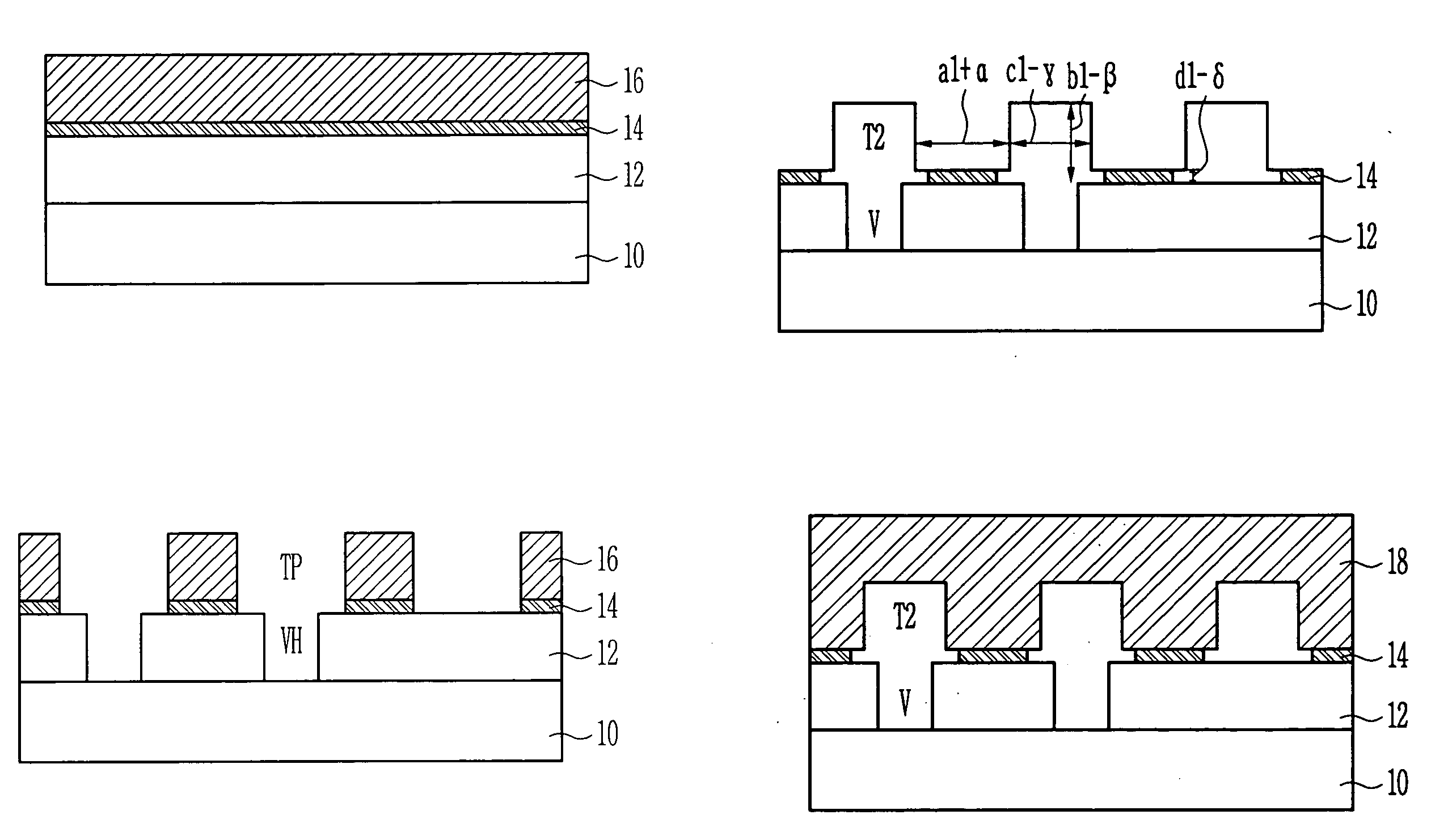
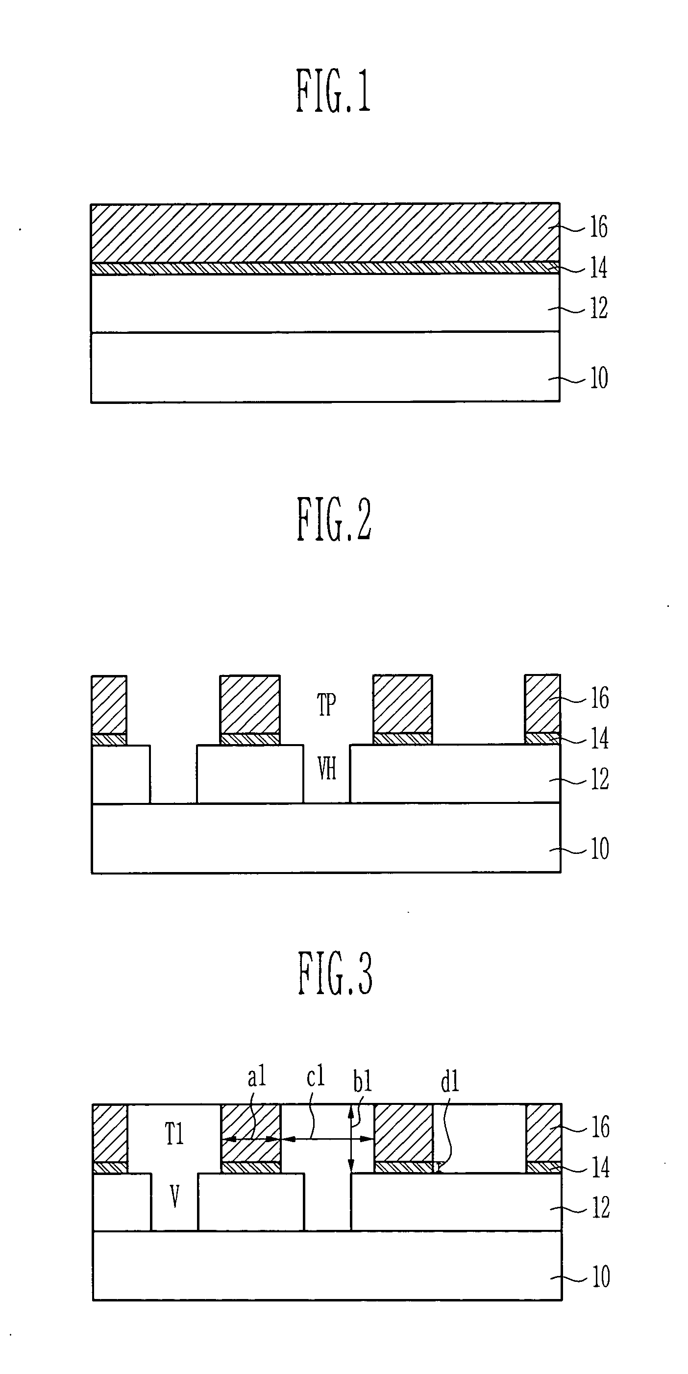
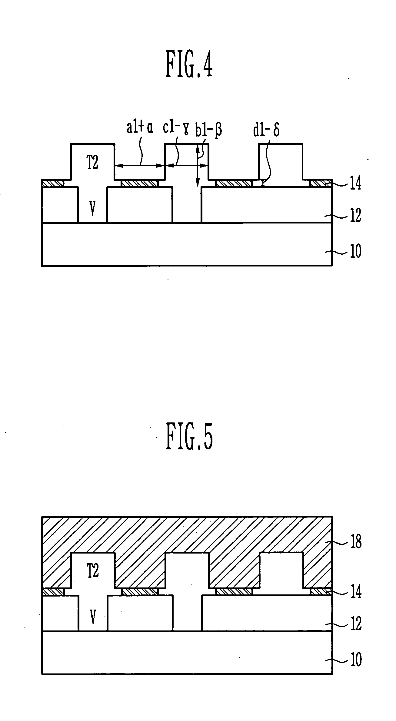
[0016] A method for forming a metal line in a semiconductor device in accordance with a preferred embodiment of the present invention will now be described in detail with reference to the accompanying drawings. In the drawings, a thickness of a film is exaggerated to emphasize clear and accurate explanations. Wherever possible, the same reference numerals will be used throughout the drawings and the description to refer to the same or like parts. In addition, in case it is described that one film is disposed on or contacts another film or a semiconductor substrate, one film can directly contact another film or the semiconductor substrate, or the third film can be positioned between them.

[0017] FIGS. 1 to 5 are cross-sectional diagrams illustrating sequential steps of the method for forming the metal line in the semiconductor device in accordance with the preferred embodiment of the present invention.

[0018] Referring to FIG. 1, a first insulation film 12, an etch barrier film 14 an...


PUM


Abstract

The present invention discloses a method for forming a metal line in a semiconductor device including the steps of: sequentially forming a first insulation film, an etch barrier film and a second insulation film on a semiconductor substrate on which the substructure has been formed; forming a plurality of via holes for exposing the substructure in different points by patterning the second insulation film, the etch barrier film and the first insulation film of the resulting structure, and forming a plurality of trench patterns respectively on the plurality of via holes by re-patterning the second insulation film and the etch barrier film of the resulting structure; forming a plurality of vias and trenches by filling a metal material in the plurality of via holes and trench patterns; removing the second insulation film; and forming a third insulation film over the resulting structure including the removed second insulation film.

Description

BACKGROUND [0001] 1. Field of the Invention [0002] The present invention relates to a method for manufacturing a semiconductor device, and more particularly to, a method for forming a metal line in a semiconductor device according to a damascene process. [0003] 2. Discussion of Related Art [0004] Recently, an insulation film for a metal line is not easily obtained due to a high integration tendency of a semiconductor device, and thus a process for forming a metal line by using a damascene process increasingly generates a short between the metal lines, namely a crosstalk. That is, in the process for forming the metal line by forming trench patterns, it is important to form the insulation film over a predetermined ratio to the metal line in the same pitch. However, the insulation film is excessively removed due to general processes such as a photoetching process, a cleaning process performed before filling a metal material, and a plariarization process performed after filling the meta...

Claims


Application Information

Patent Timeline
Patent Type & Authority Applications(United States)
IPC IPC(8): H01L21/28H01L21/306H01L21/308H01L21/3205H01L21/44H01L21/3065H01L21/4763H01L21/768H01L23/48H01L23/52H01L29/40
CPCH01L21/76892H01L21/76885H01L21/28
Inventor KIM, TAE KYUNG
Owner MICRON TECH INC
Why Eureka
Try Eureka