Wafer thinning method

A wafer and device wafer technology, applied in the field of wafer thinning, can solve the problems of reducing the quality and reliability of device wafers, reducing the utilization rate of device wafers, etc., to achieve the effect of avoiding low utilization rate and improving quality

Active Publication Date: 2012-12-19
OMNIVISION TECH (SHANGHAI) CO LTD
View PDF5 Cites 31 Cited by
  • Summary
  • Abstract
  • Description
  • Claims
  • Application Information

AI Technical Summary

Problems solved by technology

[0014] The object of the present invention is to provide a wafer thinning method to solve the problem of eliminating the height difference between the device wafer and the surf

Method used


Image

  • Wafer thinning method
  • Wafer thinning method
  • Wafer thinning method

Examples


Example Embodiment

[0039] The wafer thinning method proposed by the present invention will be further described in detail below in conjunction with the accompanying drawings and specific embodiments. Advantages and features of the present invention will be apparent from the following description and claims. It should be noted that all the drawings are in a very simplified form and use imprecise scales, and are only used to facilitate and clearly assist the purpose of illustrating the embodiments of the present invention.
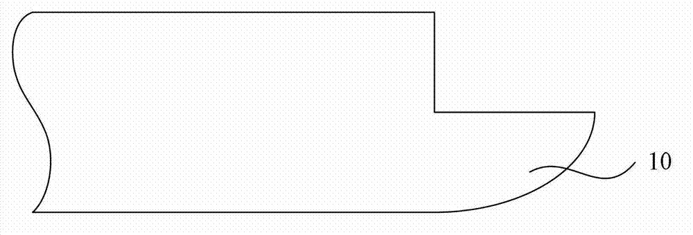
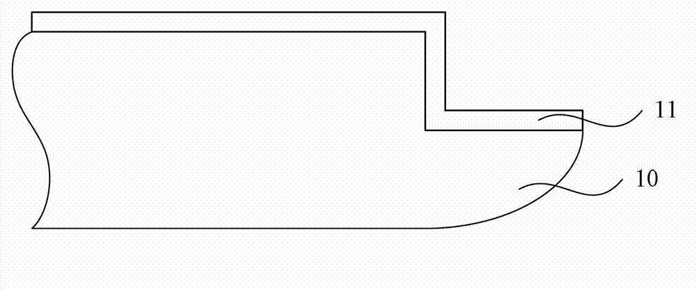
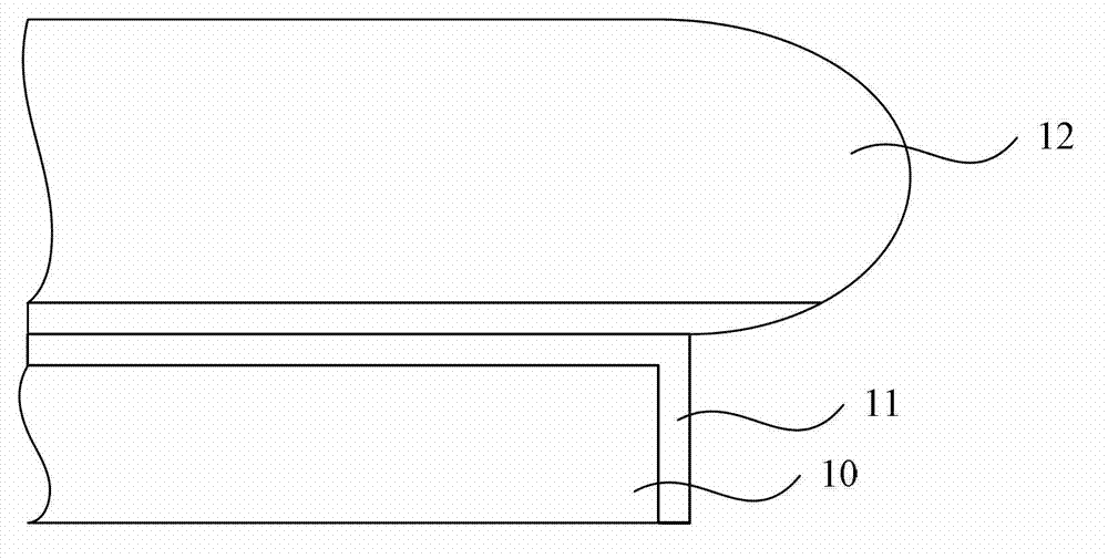
[0040] The core idea of ​​the present invention is to make use of chemical process to make up for the two etching processes of the device wafer and the device wafer's crystal edge oxide layer by using SPINETCH-D and HNA respectively. The height difference of the surface of the oxide layer at the edge of the crystal avoids the problems of low utilization rate of device wafers and low quality and reliability of device wafers produced by physical processes (ie, shearing processes...


PUM

PropertyMeasurementUnit
Thicknessaaaaaaaaaa
Thicknessaaaaaaaaaa

Abstract

The invention provides a wafer thinning method, which is characterized in that selective corrosive liquid is utilized for etching an crystal edge oxidization layer of a device wafer, wherein the etching rate of the selective corrosive liquid on the oxidization layer is larger than the etching rate on the device wafer, so that the height difference of the device wafer and a crystal edge oxidization layer surface of the device wafer by respectively utilizing SPINETCH-D (mixed solution of phosphoric, nitric acid, sulfuric acid and hydrofluoric acid) and HNA (mixed solution of hydrofluoric acid, nitric acid and acetic acid) to perform two etching process on the back surface of the device wafer and the crystal edge oxidization layer of the device wafer can be overcome. Meanwhile, by utilizing the chemical process, the problem by utilizing the physical process (i.e. cutting process) that the utilization rate of the produced device wafer is low and the quality and the reliability of the device wafer are low can be avoided, and the quality of a finally formed image sensor can be improved.

Description

technical field [0001] The invention relates to the technical field of integrated circuit manufacturing technology, in particular to a wafer thinning method in the manufacturing process of a back-illuminated sensor. Background technique [0002] The image sensor is developed on the basis of photoelectric technology. The so-called image sensor is a sensor that can sense optical image information and convert it into a usable output signal. Image sensors can improve the visual range of the human eye, enabling people to see the microcosm and macrocosm that cannot be seen by the naked eye, see what happens in places that people cannot reach temporarily, and see various physical and chemical changes beyond the visual range of the naked eye. Life, physiology, the occurrence and development of disease, and so on. It can be seen that image sensors play a very important role in people's culture, sports, production, life and scientific research. It can be said that modern human activ...

Claims


Application Information

Patent Timeline
IPC IPC(8): H01L27/146H01L21/02
Inventor 林峰洪齐元
Owner OMNIVISION TECH (SHANGHAI) CO LTD
Why Eureka
Try Eureka