Organic light emitting display and method of manufacturing the same

A light-emitting display, organic technology, applied in semiconductor/solid-state device manufacturing, electroluminescent light source, light source, etc., can solve the problems of impurity diffusion, complicated organic light-emitting display manufacturing process, and cost increase

Inactive Publication Date: 2007-12-05
SAMSUNG MOBILE DISPLAY CO LTD
View PDF0 Cites 30 Cited by
  • Summary
  • Abstract
  • Description
  • Claims
  • Application Information

AI Technical Summary

Problems solved by technology

As a result, there are problems in that the manufacturing process of the organic light emitting display is complicated and the cost is increased
However, since the N + impurity doping process, so when forming the gate electrode, the doped N + Impurities can diffuse unnecessarily
As a result, the problem is that the performance and reliability of CMOS TFTs are degraded, thereby reducing the display quality of OLEDs

Method used


Image

  • Organic light emitting display and method of manufacturing the same
  • Organic light emitting display and method of manufacturing the same
  • Organic light emitting display and method of manufacturing the same

Examples


Embodiment Construction

[0029] The present invention will now be described more fully with reference to the accompanying drawings, in which exemplary embodiments of the invention are shown. However, this invention may be embodied in many different forms and should not be construed as limited to the embodiments set forth herein. Rather, these embodiments are provided so that this disclosure will be thorough and complete, and will fully convey the concept of the invention to those skilled in the art.

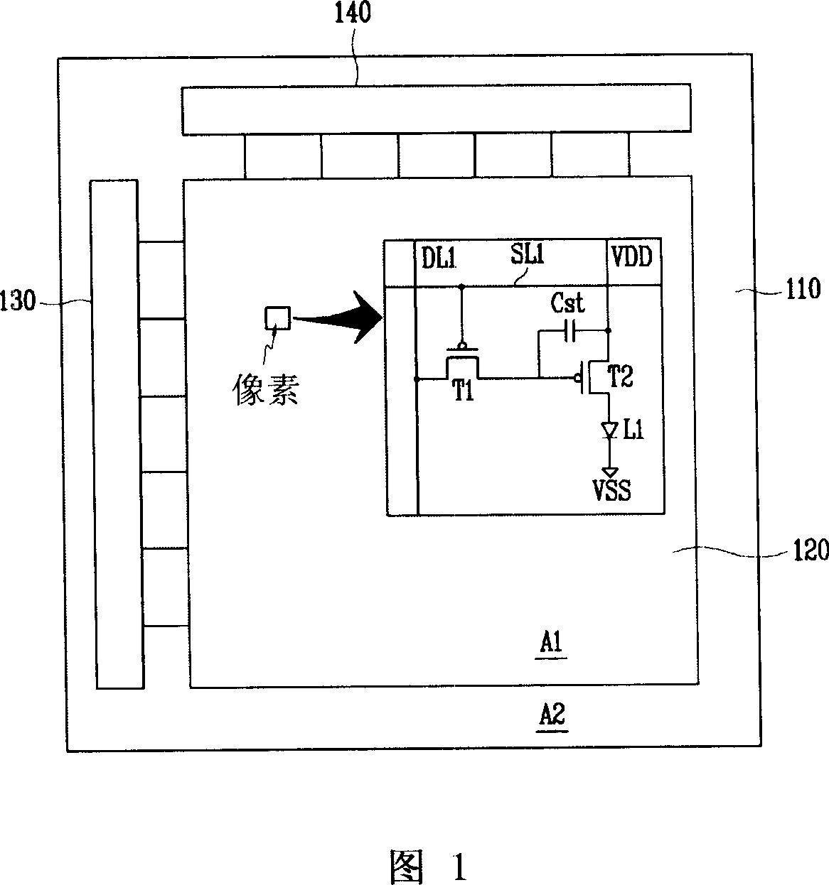
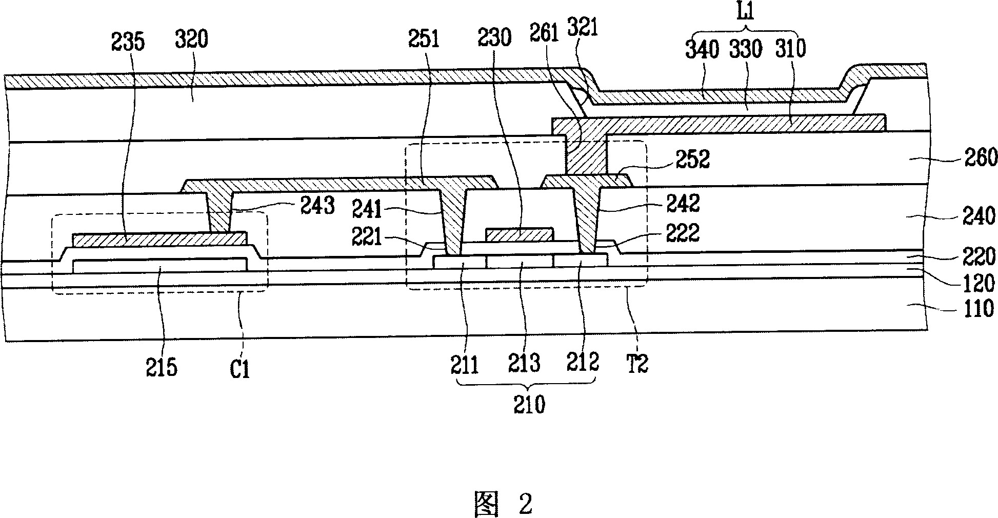
[0030] An organic light emitting display according to an embodiment of the present invention will now be described with reference to FIG. 1 and FIG. 2, FIG. 1 is a schematic diagram showing an organic light emitting display according to an embodiment of the present invention, and FIG. cutaway view.

[0031] Referring to FIG. 1 , a pixel region A1 for light emission or image representation is formed on a substrate 110 , and a non-pixel region A2 is formed on the substrate 110 around the pixel region A1 ....


PUM


Abstract

In an organic light emitting display, the process of forming a storage capacitor is simplified, and deterioration of the properties and the reliability of the TFT is prevented. The organic light emitting display includes a substrate, a thin film transistor formed on one portion of the substrate, the thin film transistor having an active layer, a gate electrode, a gate insulating layer interposed between the active layer and the gate electrode, and a storage capacitor formed on another portion of the substrate. The storage capacitor has a first electrode formed on the same surface as the active layer, and a second electrode formed on the same surface as the gate electrode, with the gate insulating layer being interposed between the first electrode and the second electrode. The active layer and the first electrode are made of an intrinsic polysilicon layer.

Description

technical field [0001] The present invention relates to an organic light emitting display, and more particularly, to an organic light emitting display having a storage capacitor and a method of manufacturing the organic light emitting display. Background technique [0002] Unlike cathode ray tubes (CRTs), which are bulky and operate with high voltage, display devices such as organic light emitting displays and liquid crystal displays are thin and operate with low voltage, which are being widely used as next generation display devices. [0003] Specifically, an organic light-emitting display is a self-emission display device in which electrons and holes injected into an organic material through an anode and a cathode recombine to generate excitons, and as a function of the energy of the generated excitons As a result, light with a specific wavelength is emitted. Therefore, since the organic light emitting display does not require a separate light source such as a backlight u...

Claims


Application Information

Patent Timeline
Patent Type & Authority Applications(China)
IPC IPC(8): H01L27/02H01L27/32H01L21/82H05B44/00
CPCH01L27/3262H01L27/3265H01L27/13H01L27/1214H01L27/12H01L27/3244H01L27/1255H01L51/56H10K59/12H10K59/1213H10K59/1216H10K71/00
Inventor 黄义勋崔雄植
Owner SAMSUNG MOBILE DISPLAY CO LTD
Why Eureka
Try Eureka