Method of exposing wafer using scan-type exposure apparatus

a scanning-type exposure and wafer technology, applied in the direction of photomechanical equipment, instruments, printers, etc., can solve the problems of productivity degradation in the exposure process, reduce the total scanning distance required, reduce the total amount of exposure time, and improve the effect of the exposure process

Inactive Publication Date: 2005-05-19
SAMSUNG ELECTRONICS CO LTD
View PDF4 Cites 8 Cited by
  • Summary
  • Abstract
  • Description
  • Claims
  • Application Information

AI Technical Summary

Benefits of technology

[0013] The present invention provides a method of exposing a wafer using a scan-type exposure apparatus, which improves productivity in an exposure process by minimizing a scanning distance of a scanner.
[0018] Each of the array of shots forming the second shot column is scan exposed in the second direction, and in the second shot column, shots that are alternatively selected from the array of shots disposed in the first direction are exposed. The method may further comprise before the scan exposing of each of the array of shots forming the second shot column, pre-scanning that starts in the first shot column and progresses in the second direction. A scanning distance in the pre-scanning may be less than or equal to a scanning distance required for the scan exposing of each of the array of shots forming the second shot column. According to the present invention, when a scanner is moved to expose the next shot after one shot is scan exposed on a wafer, a post-scanning section is removed, thereby reducing the total scanning distance required for wafer exposure when compared to conventional art. Therefore, according to an embodiment of the present invention, it is possible to reduce the total amount of time required for exposure and improve productivity in the exposure process by removing an unnecessary scanning distance in the exposure process and reducing the scanning distance required for the exposure process.

Problems solved by technology

As a result, the scanning distance for exposure and the amount of time required for exposing a semiconductor chip will substantially increase, causing degradation of productivity in the exposure process.

Method used


Image

  • Method of exposing wafer using scan-type exposure apparatus
  • Method of exposing wafer using scan-type exposure apparatus
  • Method of exposing wafer using scan-type exposure apparatus

Examples


Embodiment Construction

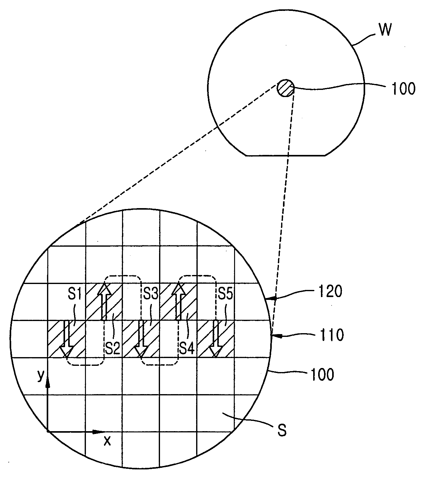
[0024] The present invention will now be described more fully with reference to the accompanying drawings, in which an embodiment of the invention is shown. Throughout the drawings, like reference numerals are used to refer to like elements. FIG. 3 is a view for explaining a method of exposing a wafer in a scan-type exposure apparatus according to a preferred embodiment of the present invention. Referring to FIG. 3, in the method of exposing a wafer W according to the present invention, a plurality of shots S formed repeatedly along a first direction (x-direction) and a second direction (y-direction) are orthogonal to each other in an exposure target area 100 on the wafer W. A first shot S1 selected from a first shot column 110 is first scan exposed. The first shot column 110 is formed of an array of shots disposed in a row in the x-direction. After the first shot S1 is scan exposed, a second shot S2 that is included in a second shot column 120 is disposed in a diagonal direction to...


PUM

PropertyMeasurementUnit
areaaaaaaaaaaa
scanning distanceaaaaaaaaaa
photosensitiveaaaaaaaaaa

Abstract

Provided is a method of exposing a wafer using a scan-type exposure apparatus. The method includes scan exposing a first shot selected from a first shot column formed of an array of shots disposed in a row in a first direction. The first shot column may be included in a plurality of shots repeatedly formed in the first direction and a second direction that are substantially orthogonal to each other in an exposure target area on the wafer. The method further includes scan exposing a second shot that is included in a second shot column and disposed in a diagonal direction to the first shot. The second shot column may be formed of an array of shots disposed in a row in the first direction and is closer to the first shot column than any other shot in the plurality of shots.

Description

BACKGROUND OF THE INVENTION [0001] This application claims the priority of Korean Patent Application No. 2003-0080575, filed on Nov. 14, 2003, in the Korean Intellectual Property Office, the disclosure of which is hereby incorporated by reference in its entirety. [0002] 1. Field of the Invention [0003] The present invention relates to a method of manufacturing a semiconductor device, and more particularly, to a method of exposing a wafer using a scan-type exposure apparatus. [0004] 2. Description of the Related Art [0005] In general, photolithographic processes are used to manufacture semiconductor devices. During the photolithographic process, a photosensitive film is coated on a wafer used to form a fine circuit pattern, a pattern of a predetermined shape formed on a mask is transferred onto the wafer by projecting light to the mask using an exposure apparatus. Thus, the pattern is formed on the wafer. [0006] Recently, a scan-type exposure apparatus that performs exposure by movin...

Claims


Application Information

Patent Timeline
Patent Type & Authority Applications(United States)
IPC IPC(8): C30B23/00C30B25/00C30B28/12C30B28/14H01L21/027G03F7/20
CPCG03F7/70358G03F7/70433G03F7/70425H01L21/027
Inventor LEE, DONG-HAN
Owner SAMSUNG ELECTRONICS CO LTD
Why Eureka
Try Eureka