Memory device and fabrication method thereof

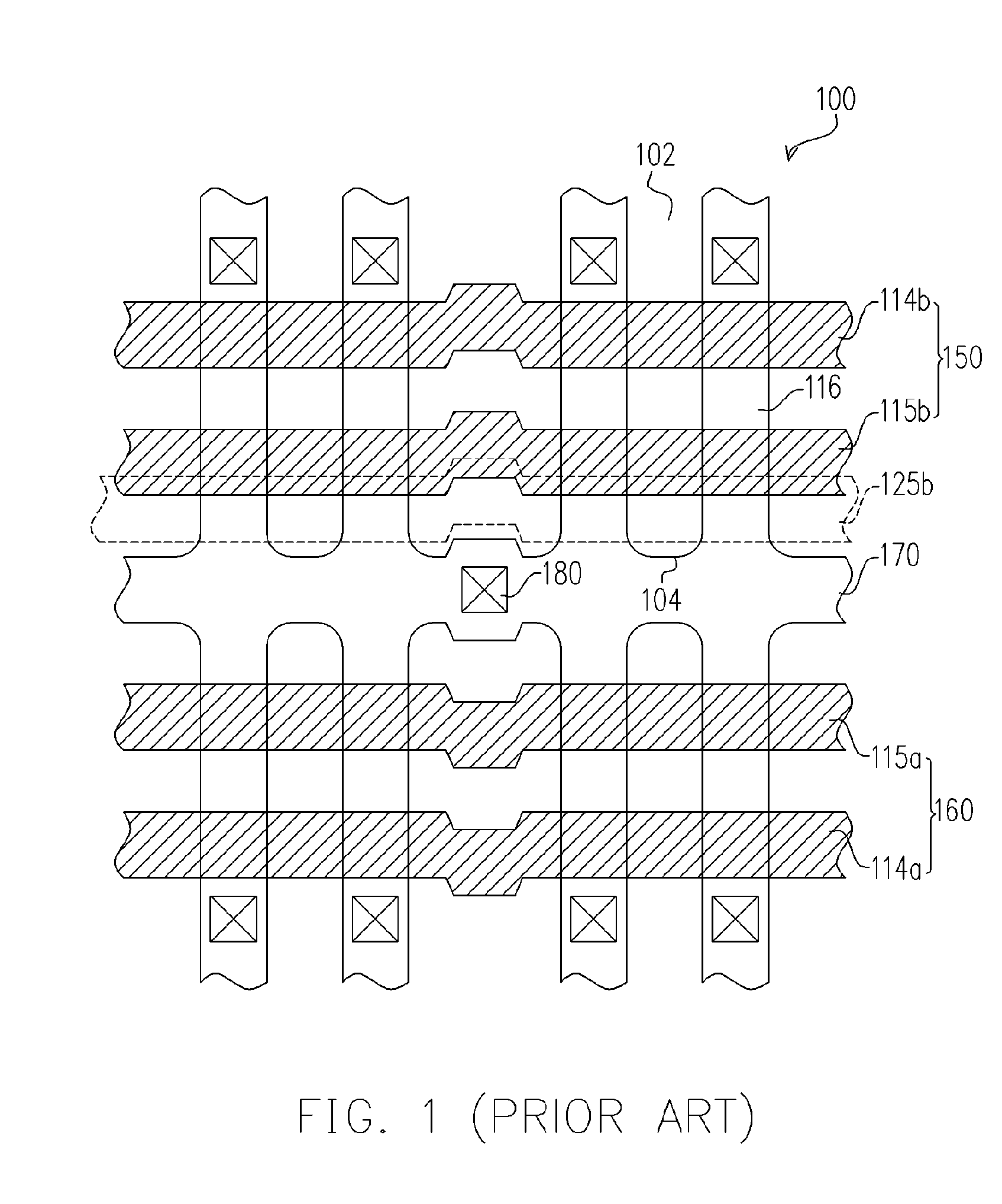
a memory device and fabrication method technology, applied in semiconductor devices, digital storage, instruments, etc., can solve the problems of consuming more chip areas, affecting the high integration of devices, and complicated fabrication processes, so as to reduce the resistance of source lines

Inactive Publication Date: 2005-05-19
SHIH CHUNG CHIN
View PDF0 Cites 5 Cited by
  • Summary
  • Abstract
  • Description
  • Claims
  • Application Information

AI Technical Summary

Benefits of technology

[0010] The invention provides a memory device and the fabrication method thereof, in which no extra contacts are required for reducing the resistance of the source line.
[0011] The invention provid

Problems solved by technology

Since an extra doping process is performed to the active region 104 of the substrate 100 to form the source line 170, the fabrication processes become more complicated and costly.
As mentioned above, the prior art flash memory structure usually occupies more chip areas and hinders high integration of the device.
However, due to ma

Method used


Image

  • Memory device and fabrication method thereof
  • Memory device and fabrication method thereof
  • Memory device and fabrication method thereof

Examples


Embodiment Construction

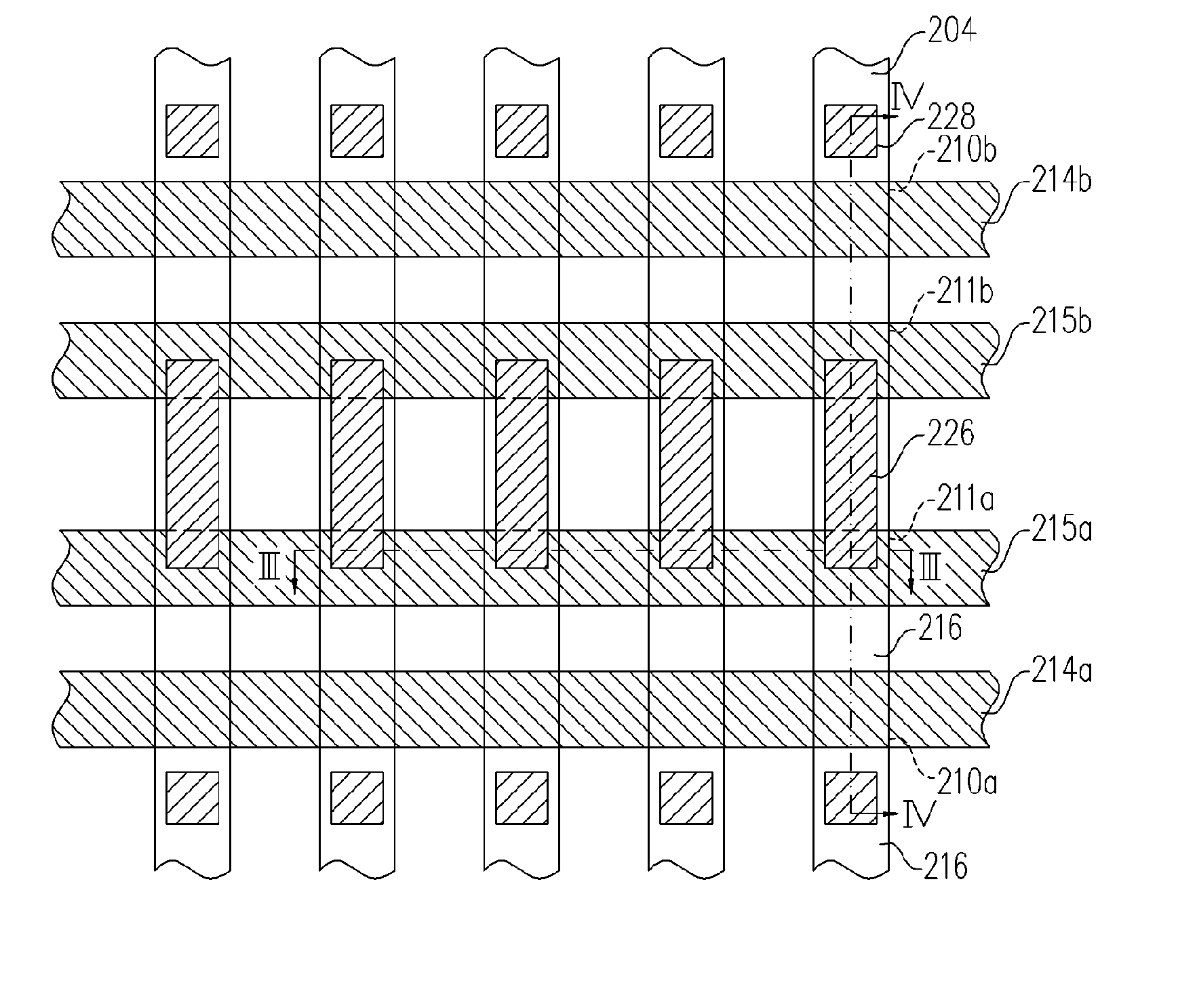
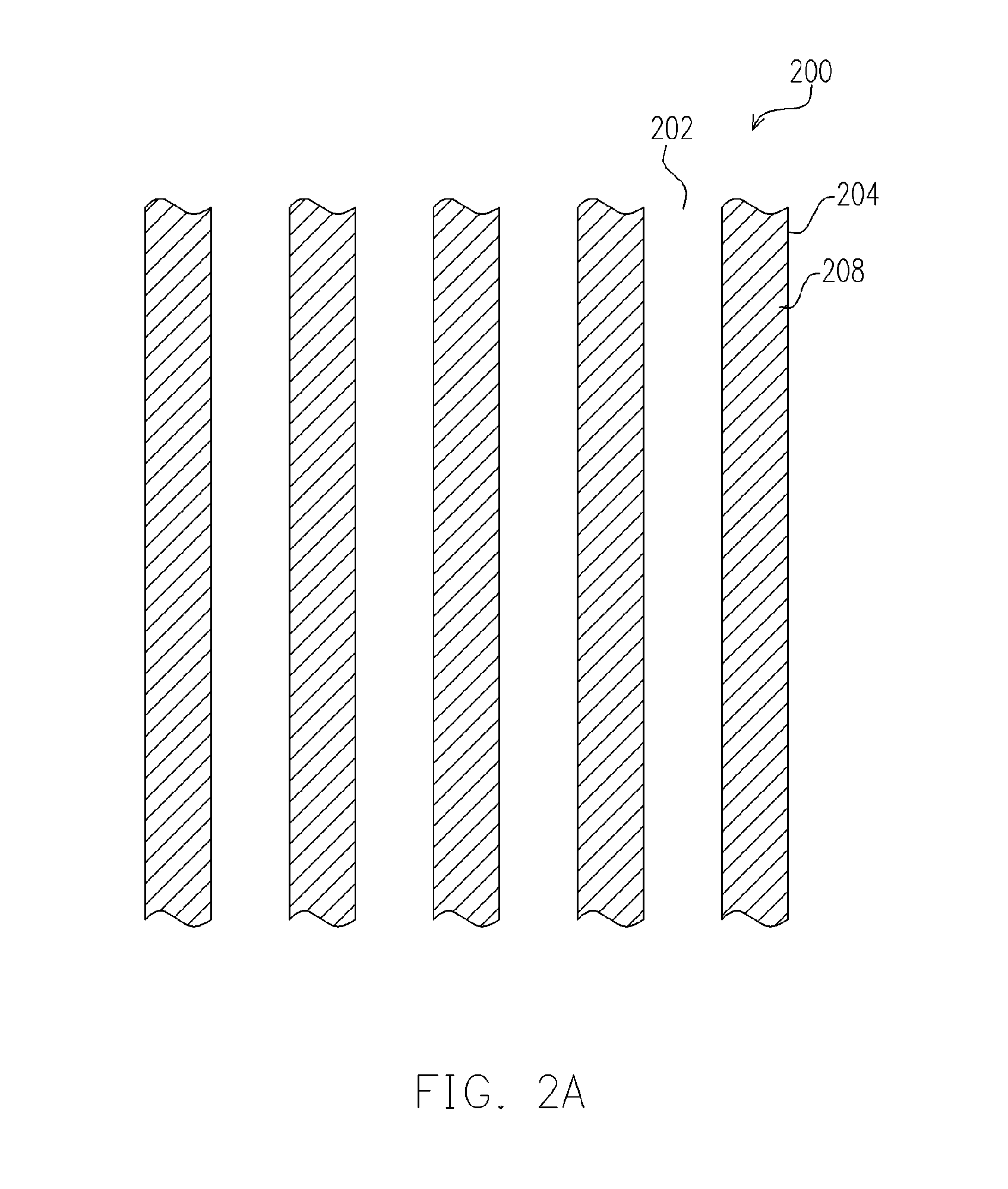
[0025]FIGS. 2A-2D are top views illustrating the process steps for forming a memory structure according to preferred embodiments of the present invention. FIGS. 3A-3D are cross-sectional views illustrating the process steps for forming the memory structure of FIGS. 2A-2D along the line III-III, according to one preferred embodiment of the present invention. FIGS. 4A-4D are cross-sectional views illustrating the process steps for forming the memory structure of FIGS. 2A-2D along the line IV-IV, according to one preferred embodiment of the present invention.

[0026] Referring to FIGS. 2A, 3A and 4A, a plurality of isolation structures 202 is formed in a substrate 200 and defines a plurality of active regions 204 in the substrate 200. The isolation structures 202 can be, for example, shallow trench isolation structures (STI). Preferably, the isolation structures 202 are in strip shapes and arranged substantially parallel to one another, so that the active regions 204 in strip shapes are...


PUM


Abstract

The present invention relates to a memory device and the fabrication method thereof. A plurality of pairs of floating gates and a plurality of pairs of select gates are formed above each active region. After forming a dielectric layer on each floating gate and on each select gate, a plurality of pairs of word lines and a plurality of pairs of source lines are formed simultaneously. The word lines and the source lines are disposed in a direction vertical to the strip active regions. A plurality of source/drain regions is disposed in the substrate beside the word lines and the source lines. After forming a thick dielectric layer over the substrate, a plurality of source line contacts are formed in the thick dielectric layer for connecting the source/drain regions that are between each pair of source lines and at least connecting one of each pair of the source lines.

Description

CROSS-REFERENCE TO RELATED APPLICATION [0001] This application is a divisional of a prior application Ser. No. 10 / 707,016, filed Nov. 14, 2003.BACKGROUND OF THE INVENTION [0002] 1. Field of Invention [0003] The present invention relates to a semiconductor device and the fabrication method thereof. More particularly, the present invention relates to a memory device and the fabrication method thereof. [0004] 2. Description of Related Art [0005] The flash memory device allows multiple and repetitive writing, reading and erasure operations, and the storage data are retained even after the power supply is discontinued. Because of the aforementioned advantages, the flash memory has become the mainstream non-volatile memory device, which is widely applied in the electronic products, such as, personal computers, digital cameras and personal digital assistants (PDAs) etc. [0006] At present, the commonly adopted flash memory cell is composed of a stacked gate consisting of a floating gate and...

Claims


Application Information

Patent Timeline
IPC IPC(8): G11C11/34H01L21/336H01L21/8247H01L27/108H01L27/115
CPCH01L27/115H01L27/11524H01L27/11521H01L27/11519H10B69/00H10B41/10H10B41/30H10B41/35
Inventor SHIH, CHUNG-CHIN
Owner SHIH CHUNG CHIN
Why Eureka
Try Eureka