
Memory device and method for writing data in memory cell with boosted bitline voltage

a memory cell and bitline voltage technology, applied in the field of memory devices, can solve the problem of the capacitance limit of each cell capacitor, and achieve the effect of boosting voltage, increasing the amount of electric charge stored in the memory cell capacitor, and increasing the voltage level

Inactive Publication Date: 2005-05-19
SAMSUNG ELECTRONICS CO LTD
View PDF0 Cites 5 Cited by
  • Summary
  • Abstract
  • Description
  • Claims
  • Application Information

AI Technical Summary

Benefits of technology

[0014] In one embodiment, in step (f), the power supply voltage level of the memory device is applied to the isolation transistors between the bitline and the sense amplification unit. The isolation transistors can be turned off when the input data is at a logic high level. The isolation transistors can be turned on when the input data is at a logic low level, and then the boosted voltage of the bitline can be dropped to a ground voltage level by the sense amplification unit. According to another aspect of the present invention, there is provided a memory device. The memory device includes wordlines, which are connected to gates of memory cell transistors; bitlines, which are connected to drains of the memory cell transistors; memory cell capacitors, which are connected to sources of the memory cell transistors; a write boosting signal generation circuit, which generates a write boosting signal in response to a write command, a bitline precharge signal, and a block decoding signal, the block decoding signal selecting a memory cell array including a given memory cell transistor; and capacitors, which are connected between the bitlines and the write boosting signal.
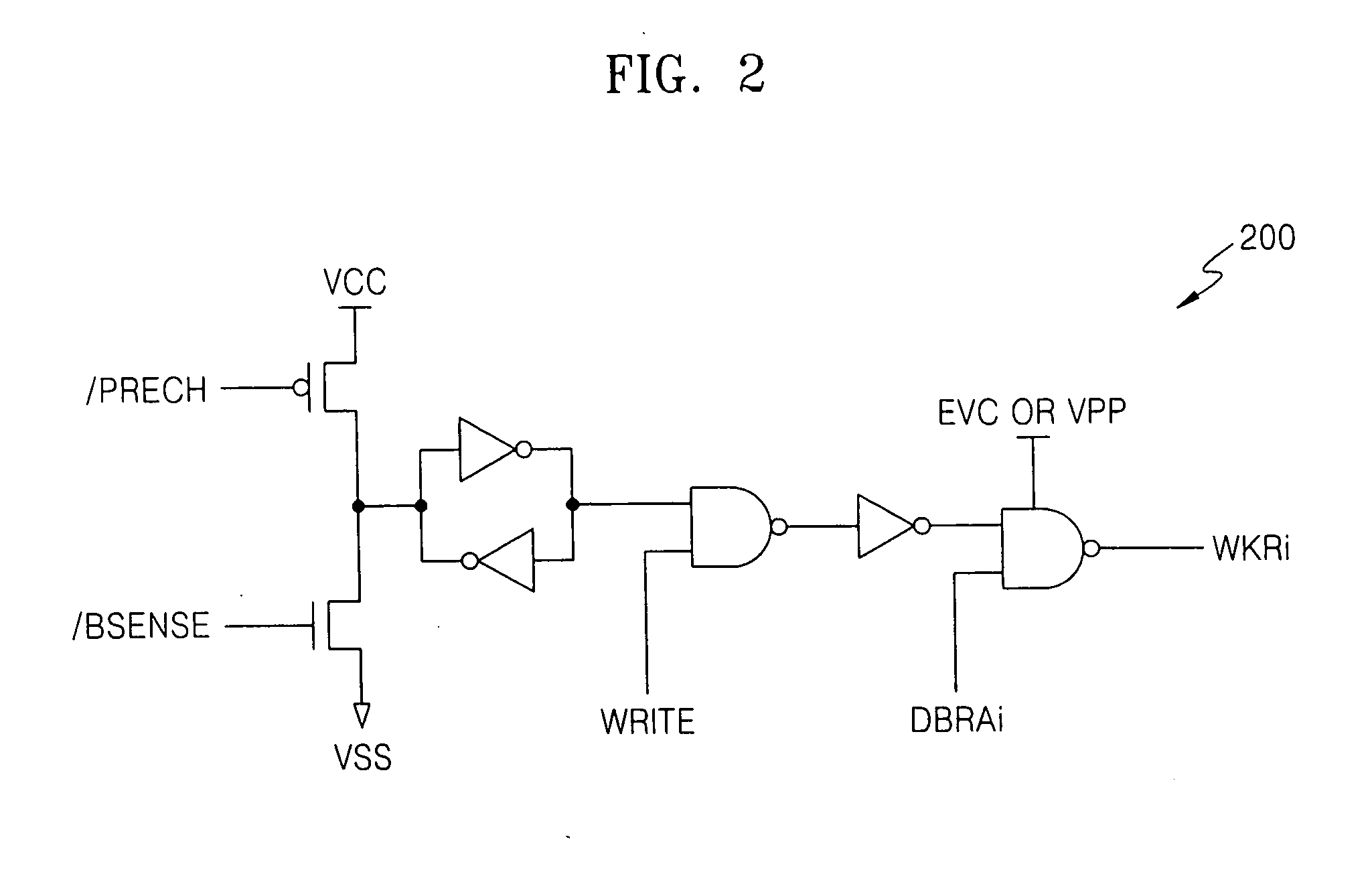
[0015] The write boosting signal generation circuit may include a PMOS transistor, a source of which is connected to a power supply voltage and a gate of which is connected to the bitline precharge signal; an NMOS transistor, a source of which is connected to a ground voltage, a gate of which is connected to a bitline sensing signal, and a drain of which is connected to a drain of the PMOS transistor; a latch unit, which is connected to the drains of the PMOS transistor and the NMOS transistor; a first NAND gate, which receives an output of the latch unit and the write command; an inverter, which inverts an output of the NAND gate; and a second NAND gate, which is driven by a boosted voltage or an external power supply voltage higher than the power supply voltage, the second NAND gate outputting the write boosting signal in response to an output of the inverter and the block decoding signal.
[0016] In one embodiment, the memory device further includes: a sense amplification unit, which senses and amplifies a voltage of each of the bitlines; and an isolation transistor, which is located between the bitline and the sense amplification unit, the transistor being gated by a bitline isolation signal. The bitline isolation signal can have a boosted voltage level, when data is written into each of the memory cell capacitors with the write boosting signal inactivated, and can have a power supply voltage level, when data is written into each of the memory cell capacitors with the write boosting signal activated. Therefore, according to the present invention, the amount of electric charge stored in a memory cell capacitor increases because the memory cell capacitor is charged, via a bitline, with a higher voltage level than a power supply voltage level. The memory cell capacitor is charged with a higher voltage level during a write boosting operation that is performed in response to a write boosting signal.

Problems solved by technology

However, since there are numerous restrictions placed on increasing the size of a chip or manufacturing a semiconductor device, there is a clear limit as to the amount by which the capacitance of each of the cell capacitors can be increased.

Method used


Image

  • Memory device and method for writing data in memory cell with boosted bitline voltage
  • Memory device and method for writing data in memory cell with boosted bitline voltage
  • Memory device and method for writing data in memory cell with boosted bitline voltage

Examples


Embodiment Construction

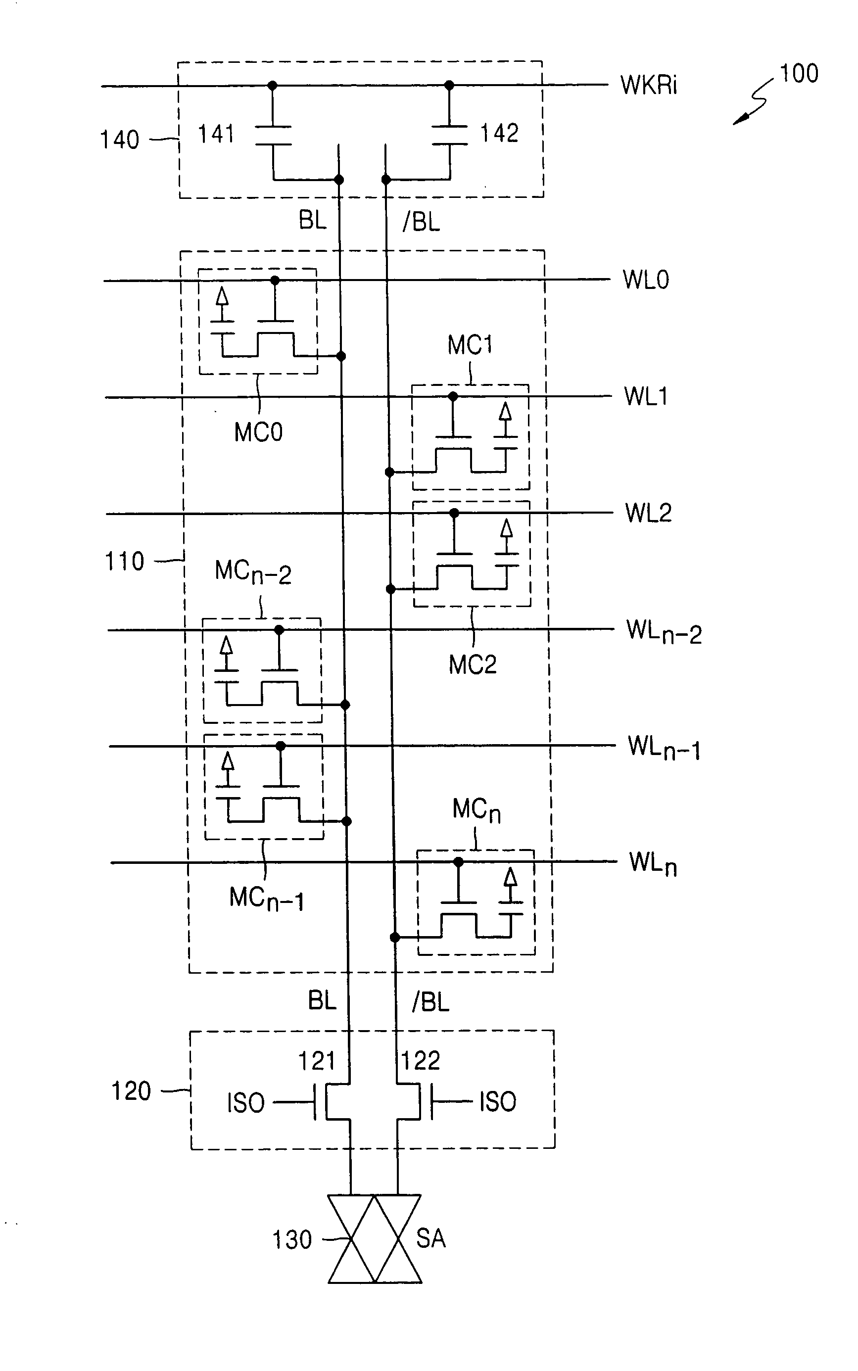
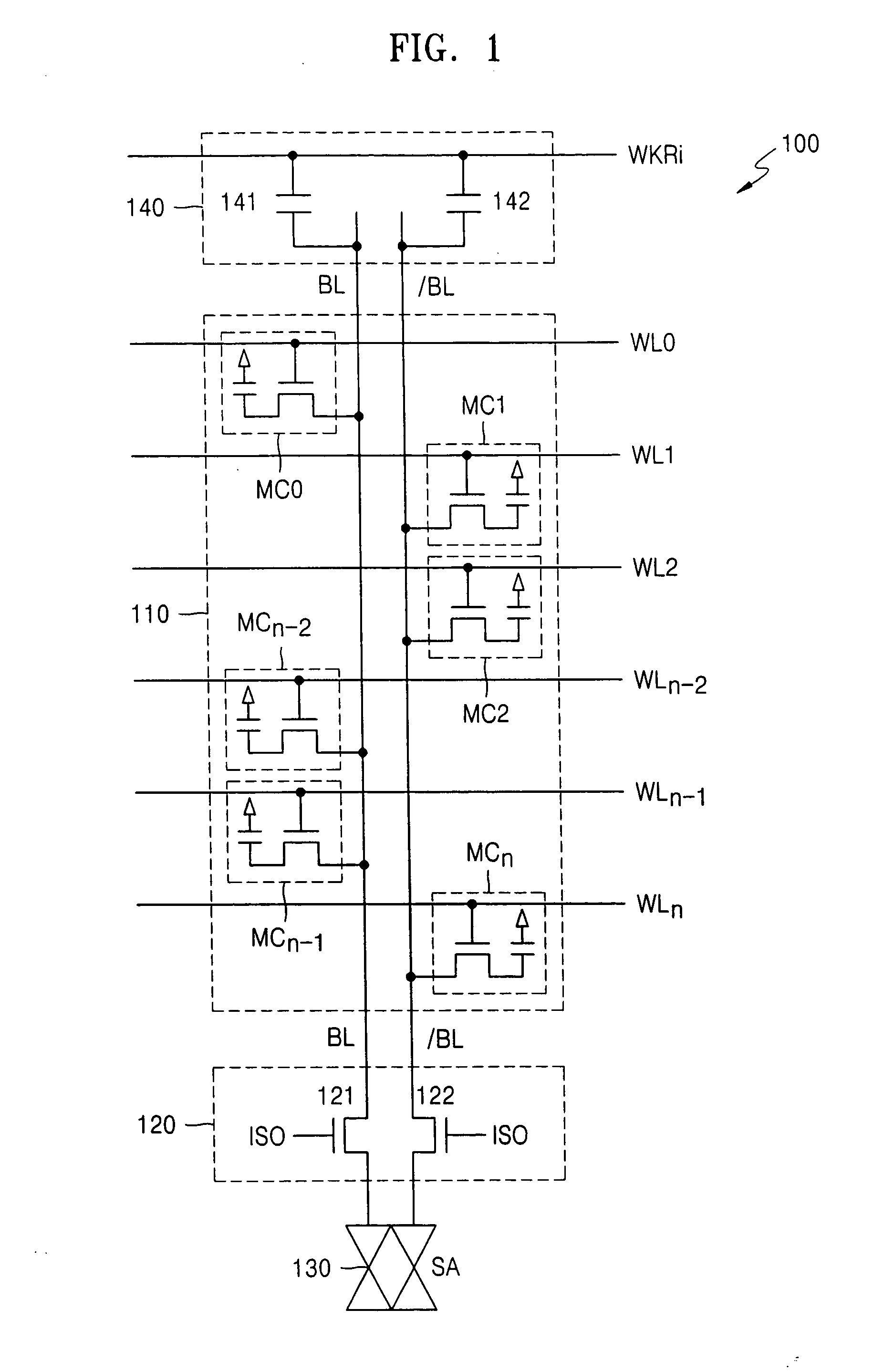
[0021]FIG. 1 is a circuit diagram illustrating the structure of a bitline pair of a memory device 100 according to an embodiment of the present invention. Referring to FIG. 1, the memory device 100 includes a memory cell array 110, a bitline isolation unit 120, a sense amplification unit 130, and a bitline capacitor unit 140. In the memory cell array unit 110, memory cells MC0, MC1, MC2, MCn-2, MCn-1, and MCn are arranged at intersection points between a wordline WL0 and a bitline BL, between a wordline WL1 and a complementary bitline / BL, between a wordline WL2 and the complimentary bitline / BL, between a wordline WLn-2 and the bitline BL, between a wordline WLn-1 and the bitline BL, and between a wordline WLn and the complementary bitline / BL, respectively. The bitline isolation unit 120 selectively connects the bitline BL or the complementary bitline / BL to the sense amplification unit 130 via a transistor 121 or 122. The transistors 121 and 122 respond to a bitline isolation sig...


PUM


Abstract

Provided are a method of writing data into a memory cell with a boosted write voltage and a memory device that performs the method. The method involves (a) transmitting data input in response to a write command to a bitline; (b) writing the input data on the bitline into a memory cell capacitor via a memory cell transistor; (c) generating a write boosting signal in response to the write command and a bitline precharge signal; (d) boosting a voltage of a capacitor connected between the write boosting signal and the bitline in response to the write boosting signal; (e) boosting a voltage of the bitline to a predetermined level; and (f) rewriting the input data into the memory cell capacitor with the boosted voltage of the bitline.

Description

BACKGROUND OF THE INVENTION [0001] This application claims the priority of Korean Patent Application No. 2003-75815, filed on Oct. 29, 2003, in the Korean Intellectual Property Office, the contents of which are incorporated herein in their entirety by reference. [0002] 1. Field of the Invention [0003] The present invention relates to a semiconductor memory device, and more particularly, to a method of writing data into a memory cell with a boosted bitline voltage, which is higher than a power supply voltage, and a memory device that performs the method. [0004] 2. Description of the Related Art [0005] A dynamic random access memory (DRAM) includes memory cells, and each of the memory cells is comprised of a transistor and a capacitor. Each of the memory cells, i.e., DRAM cells, stores a logic data value of “1” or “0” according to the amount of electric charge stored in its memory cell capacitor. In general, a data value of 1 is stored in a DRAM cell with a power supply voltage level ...

Claims


Application Information

Patent Timeline
Patent Type & Authority Applications(United States)
IPC IPC(8): G11C7/00G11C11/409G11C7/12G11C7/22G11C11/00G11C11/4076G11C11/4094
CPCG11C7/12G11C7/22G11C2207/229G11C11/4094G11C11/4076G11C11/409
Inventor CHUNG, IN-YOUNG
Owner SAMSUNG ELECTRONICS CO LTD
Learn More