Anti-blooming storage pixel

a technology of storage pixel and pixel cell, which is applied in the field of semiconductor devices, can solve the problems of pixel cell error called blooming, pixel cell saturated, and inability to hold all of the charge generated by the photo-conversion device, and achieves high signal-to-noise ratio, high dynamic range, and increased storage capacity

Active Publication Date: 2005-05-26
APTINA IMAGING CORP
View PDF9 Cites 141 Cited by
  • Summary
  • Abstract
  • Description
  • Claims
  • Application Information

AI Technical Summary

Benefits of technology

[0008] Exemplary embodiments of the present invention address the above described problems and provide pixel cells with increased storage capacity that are capable of anti-blooming operations resulting in high signal to noise ratio and high dynamic range. In an exemplary embodiment a pixel cell has an electronic shutter that transfers charge generated by a photo-conversion device to a storage node before further transferring the charge to the...

Problems solved by technology

Imager pixel cells, including CMOS imager pixel cells, typically have low signal to noise ratios and narrow dynamic range because of their inability to filly collect, transfer, and store the fill extent of electric charge generated by the photosensitive area of the photo-conversion device.
Another source of pixel cell error is called blooming.
Blooming is caused when too much light...

Method used


Image

  • Anti-blooming storage pixel
  • Anti-blooming storage pixel
  • Anti-blooming storage pixel

Examples


Embodiment Construction

[0024] In the following detailed description, reference is made to the accompanying drawings, which form a part hereof and illustrate specific embodiments in which the invention may be practiced. In the drawings, like reference numerals describe substantially similar components throughout the several views. These embodiments are described in sufficient detail to enable those skilled in the art to practice the invention, and it is to be understood that other embodiments may be utilized, and that structural, logical and electrical changes may be made without departing from the spirit and scope of the present invention.

[0025] The terms “wafer” and “substrate” are to be understood as including silicon, silicon-on-insulator (SOI), or silicon-on-sapphire (SOS) technology, doped and undoped semiconductors, epitaxial layers of silicon supported by a base semiconductor foundation, and other semiconductor structures, as well as insulating substrates, such as quartz or glass. Furthermore, whe...


PUM


Abstract

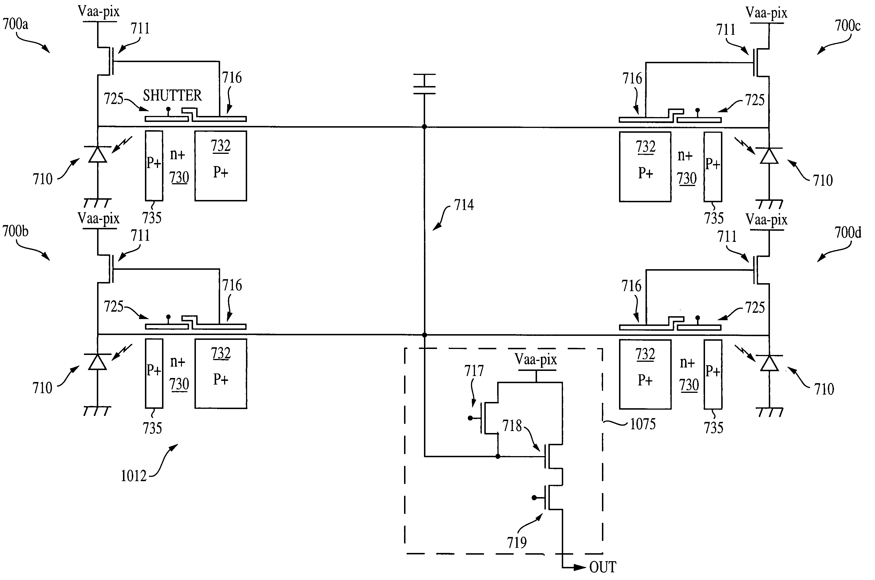
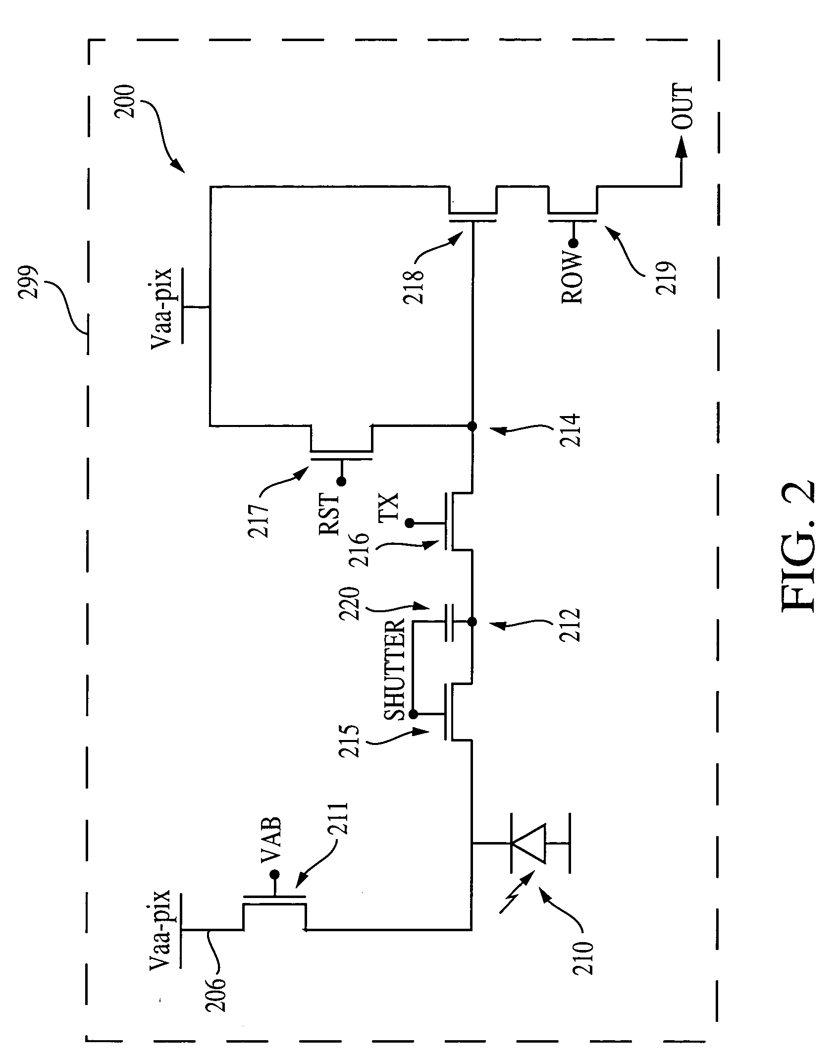
Embodiments of the present invention provide pixel cells with increased storage capacity, which are capable of anti-blooming operations. In an exemplary embodiment a pixel cell has an electronic shutter that transfers charge generated by a photo-conversion device to a storage node before further transferring the charge to the pixel cell's floating diffusion node. Each pixel cell also includes an anti-blooming transistor for directing excess charge out of each respective pixel cell, thus preventing blooming. Additionally, two or more pixel cells of an array may share a floating diffusion node and reset and readout circuitry.

Description

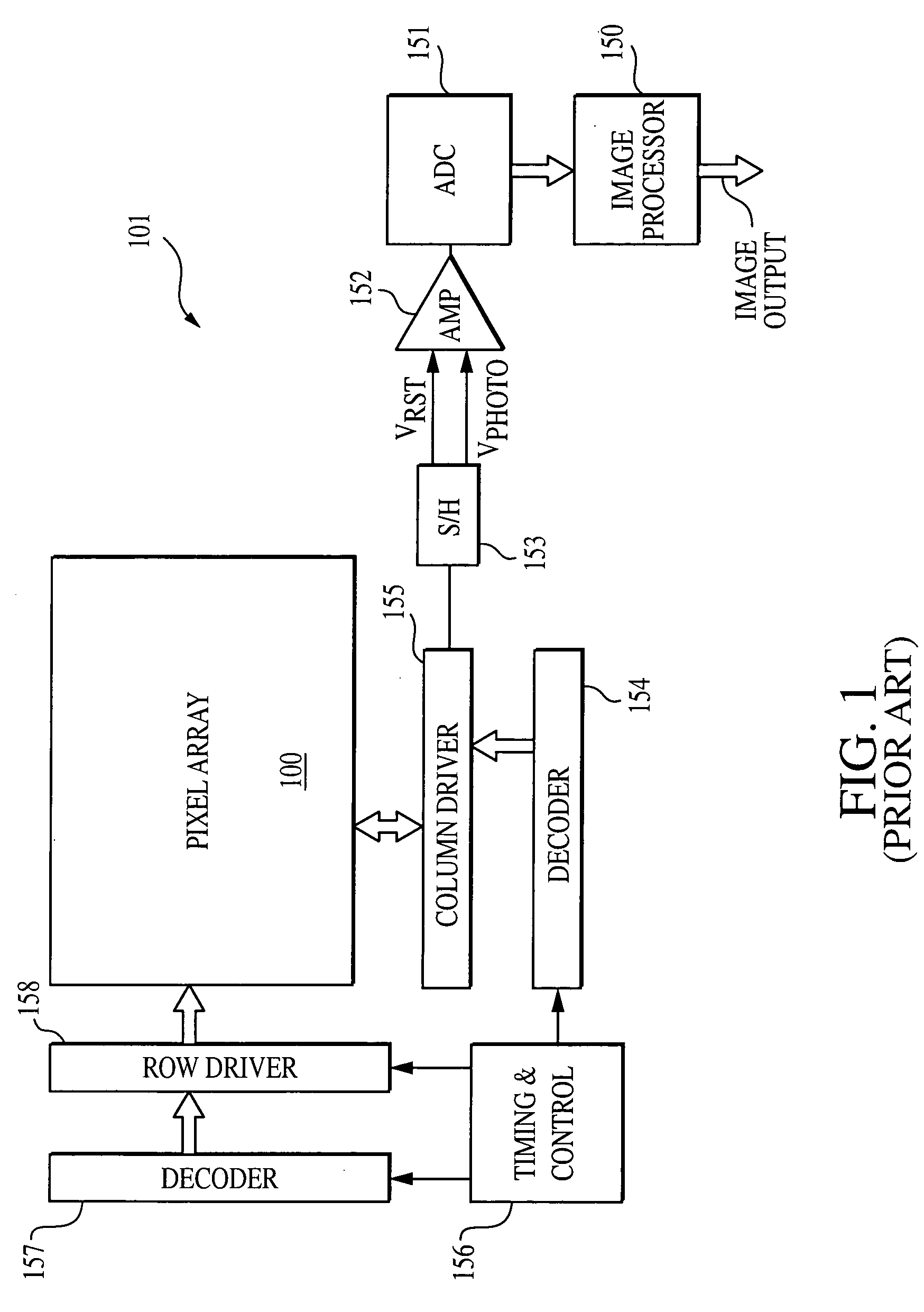
FIELD OF THE INVENTION [0001] The present invention relates to the field of semiconductor devices, particularly to an imager having improved storage capacity and blooming control. BACKGROUND OF THE INVENTION [0002] An imager, for example, a complementary metal oxide semiconductor (CMOS) imager, includes a focal plane array of pixel cells; each cell includes a photo-conversion device, for example, a photogate, photoconductor or a photodiode overlying a substrate for producing a photo-generated charge in a doped region of the substrate. A readout circuit is provided for each pixel cell and includes at least a source follower transistor and a row select transistor for coupling the source follower transistor to a column output line. The pixel cell also typically has a floating diffusion node, connected to the gate of the source follower transistor. Charge generated by the photo-conversion device is sent to the floating diffusion node. The imager may also include a transistor for transfe...

Claims


Application Information

Patent Timeline
IPC IPC(8): H01L27/146H01L29/04H04N3/15
CPCH01L27/14609H01L27/14654H01L27/14641H04N5/37457H04N5/3592H04N25/622H04N25/778
Inventor ALTICE, PETER P. JR.MCKEE, JEFFREY A.
Owner APTINA IMAGING CORP
Why Eureka
Try Eureka