Finger biometric sensor with sensor electronics distributed over thin film and monocrystalline substrates and related methods

Active Publication Date: 2005-05-26
APPLE INC
View PDF28 Cites 135 Cited by
  • Summary
  • Abstract
  • Description
  • Claims
  • Application Information

AI Technical Summary

Benefits of technology

[0010] This and other objects, features, and advantages in accordance with the present invention are provided by a finger biometric sensor which may include a thin film substrate, a thin film transistor (TFT) layer on the thin film substrate, and an array of electric field sensing electrodes adjacent the TFT layer for receiving a finger adjacent thereto. The TFT layer may include a plurality of TFTs defining a respective TFT amplifier stage for each electric field sensing electrode. The sensor

Problems solved by technology

Electronic fingerprint sensors, however, generally cannot be made smaller than the area of the finger skin that needs to be imaged.
The only result of smaller component geometrie

Method used


Image

  • Finger biometric sensor with sensor electronics distributed over thin film and monocrystalline substrates and related methods
  • Finger biometric sensor with sensor electronics distributed over thin film and monocrystalline substrates and related methods
  • Finger biometric sensor with sensor electronics distributed over thin film and monocrystalline substrates and related methods

Examples


Example

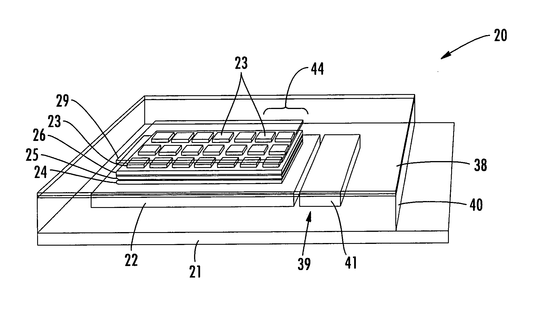
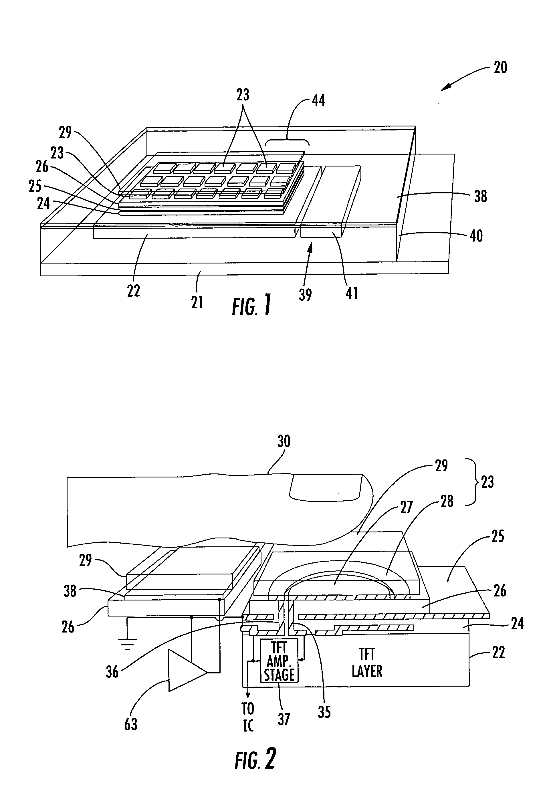
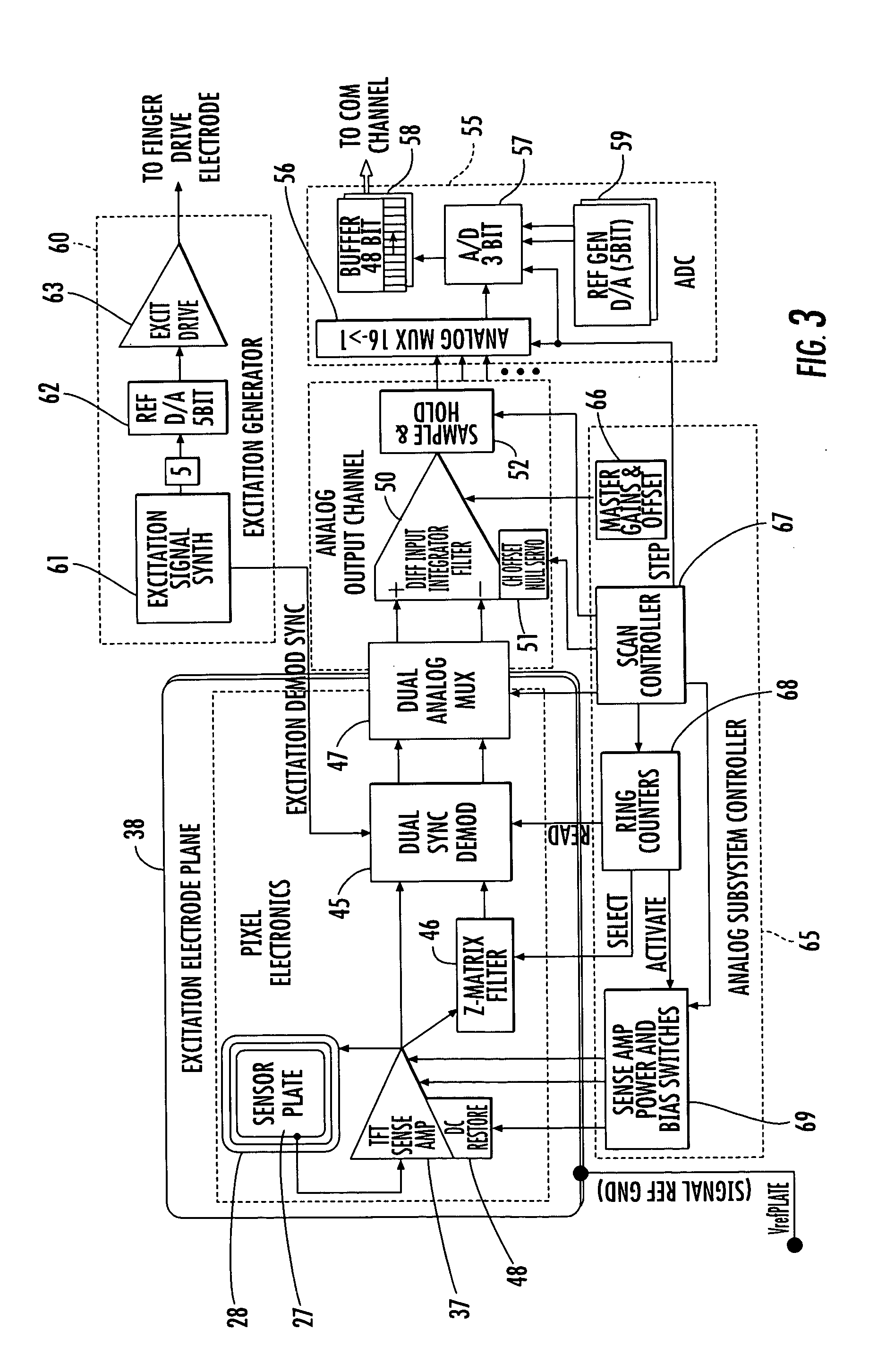
[0023] The present invention will now be described more fully hereinafter with reference to the accompanying drawings, in which preferred embodiments of the invention are shown. This invention may, however, be embodied in many different forms and should not be construed as limited to the embodiments set forth herein. Rather, these embodiments are provided so that this disclosure will be thorough and complete, and will fully convey the scope of the invention to those skilled in the art. Like numbers refer to like elements throughout, and prime and multiple prime notation is used to indicate similar elements in alternate embodiments.

[0024] Generally speaking, the present invention is directed to an approach for designing finger biometric sensors in which relatively low cost platen structures are used to partition the requisite circuitry across several different substrates. That is, a relatively low cost platen die is used for the finger sensing structures and related circuitry, and a...


PUM


Abstract

A finger biometric sensor may include a thin film substrate, a thin film transistor (TFT) layer on the thin film substrate, and an array of electric field sensing electrodes adjacent the TFT layer for receiving a finger adjacent thereto. The TFT layer may include a plurality of TFTs defining a respective TFT amplifier stage for each electric field sensing electrode. The sensor may further include a finger excitation electrode adjacent the array of electric field sensing electrodes, and at least one integrated circuit adjacent the thin film substrate. The integrated circuit may include a monocrystalline substrate and processing circuitry adjacent the monocrystalline substrate and connected to the TFT amplifier stages.

Description

CROSS-REFERENCE TO RELATED APPLICATIONS [0001] This application claims the benefit of U.S. Provisional Application No. 60 / 505,659, filed Sep. 24, 2003, which is hereby incorporated herein in its entirety by reference.FIELD OF THE INVENTION [0002] The present invention relates to the field of personal identification and verification, and, more particularly, to fingerprint sensing and processing. BACKGROUND OF THE INVENTION [0003] Fingerprint sensing and matching is a reliable and widely used technique for personal identification or verification. In particular, a common approach to fingerprint identification involves scanning a sample fingerprint or an image thereof and storing the image and / or unique characteristics of the fingerprint image. The characteristics of a sample fingerprint may be compared to information for reference fingerprints already in a database to determine proper identification of a person, such as for verification purposes. [0004] In recent years it has been prac...

Claims


Application Information

Patent Timeline
IPC IPC(8): G06K9/00H01L27/01
CPCG06K9/0002G06V40/1306
Inventor SETLAK, DALE R.
Owner APPLE INC
Why Eureka
Try Eureka