Electronics circuit manufacture

Inactive Publication Date: 2005-05-26
BJORBELL STEN
View PDF24 Cites 111 Cited by
  • Summary
  • Abstract
  • Description
  • Claims
  • Application Information

AI Technical Summary

Benefits of technology

[0021] Thus, by virtue of the internal material flowing the component is completely encapsulated without voids and without need to provide components of a particular height. Another major advant

Problems solved by technology

A disadvantage of this technique is the complexity of forming the cavities to the required dimensions.
Disadvantages of this method are that the chips must be accurately thinned and the apertures made to precisely fit the chips.
Also, it appears

Method used


Image

  • Electronics circuit manufacture
  • Electronics circuit manufacture
  • Electronics circuit manufacture

Examples


Embodiment Construction

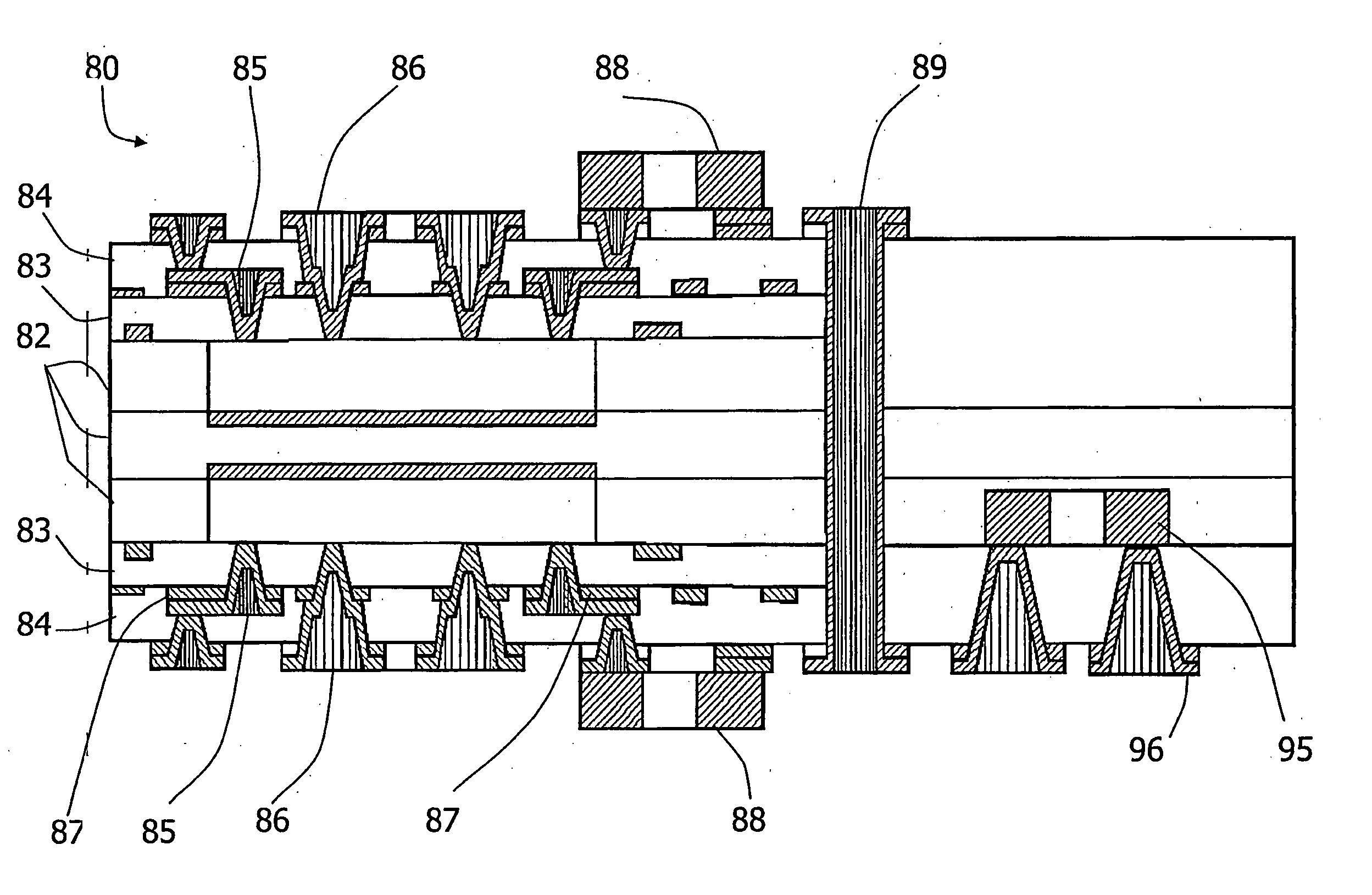
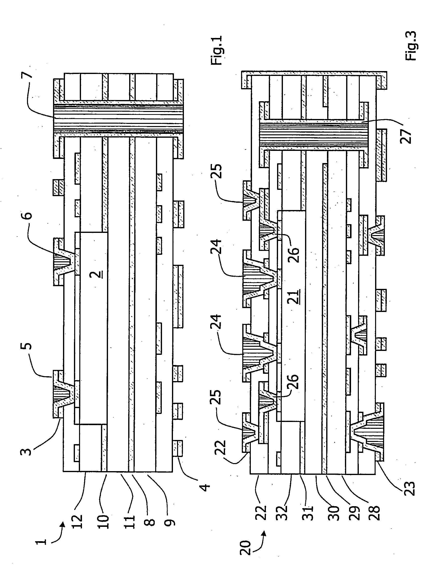
[0065] Referring to FIG. 1, a circuit 1 has an SMT component 2 embedded within a multi-layer circuit having a top foil 3 and a bottom foil 4. The component 2 is connected to the remainder of the circuit by laser-drilled vias 5 and 6 which extend from the top surface, through the foil 3 and terminate at terminals at the top of the component 2. A through via 7 extends fully through the circuit 1. All of the vias are laser-drilled and electroplated using a conventional electroplating technique.

[0066] The multi-layer board comprises FR4 layers 9, 11, and 12 and circuit conductors 8 and 10 on the FR4 layers 9 and 11. The board is manufactured in the conventional manner for multi-layer circuit boards using FR4 prepreg and FR4 material. However, the manufacturing process also embeds the component 2 into the top layer 12.

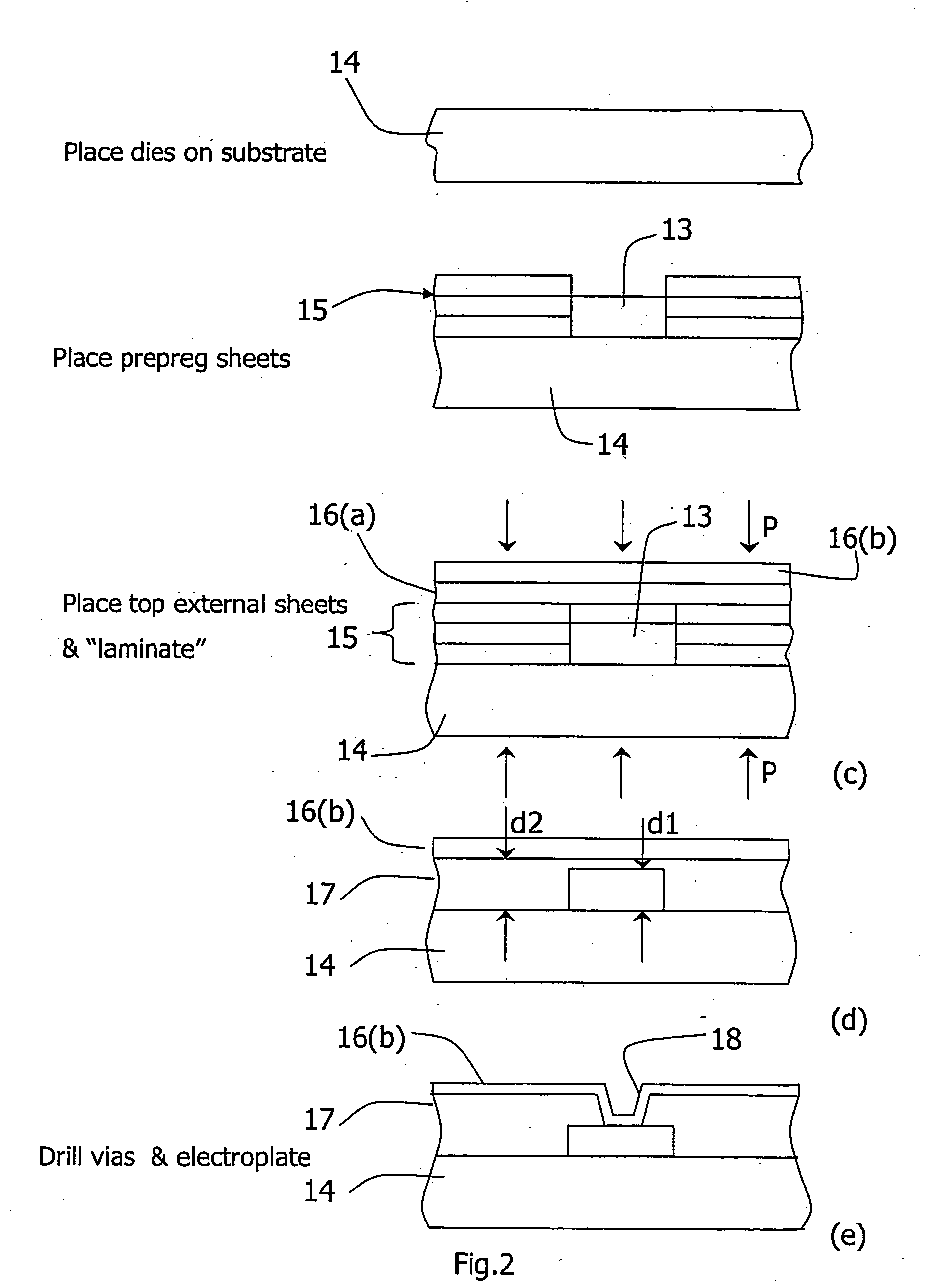
[0067] Referring to FIGS. 2(a) to 2(e) the process for embedding a component (semiconductor die) is described. For clarity, the process steps are described for a simple s...


PUM


Abstract

A circuit with embedding components (13) is produced by placing the components (13) on a substrate (14) and applying sheets (15) of prepreg. The prepreg sheets (15) have apertures to accommodate the -components, the number of sheets and arrangement of apertures being chosen to accommodate a variety of component X, Y and Z dimensions. A top layer with Cu foil (16(b)) is applied. The assembly is pressed in an operation analogous to conventional multilayer board lamination pressing. This causes all of the prepreg resin to flow to completely embed the components without raids or damage. Electrical connections are made by drilling and plating vias.

Description

INTRODUCTION [0001] 1. Field of the Invention [0002] The invention relates to manufacture of circuits having passive components such as resistors and capacitors and / or active components such as transistors and integrated circuits either packaged or unpackaged (die form). [0003] 2. Prior Art Discussion [0004] U.S. Pat. No. 6,400,573 B1 (Texas Instruments Inc.) pertains to packaging of semiconductor components and more particularly to packaging of multiple semiconductor die in a laminated substrate with an interconnect layer formed in a deposited overlay structure. Cavities of specific depths are made in the upper surface of a polymer substrate to accommodate integrated circuit chips such that the top surface of the chip and the top surface of the substrate are coplanar. A layer of laminate film is then disposed on top of the die and substrate surfaces with via openings. The via openings are disposed such that they expose bonding pads on the die surface. A conductor pattern is dispose...

Claims


Application Information

Patent Timeline
IPC IPC(8): H01L21/98H01L23/538H01L25/065H05K1/02H05K1/18H05K3/46
CPCH01L23/5385H01L23/5389H01L2924/10253H01L24/24H01L24/82H01L25/0657H01L25/50H01L2224/24227H01L2224/82039H01L2224/82047H01L2225/06524H01L2225/06541H01L2924/01013H01L2924/01029H01L2924/01075H01L2924/01078H01L2924/01082H01L2924/14H01L2924/19041H01L2924/19043H01L2924/3025H05K1/0206H05K1/185H05K3/4602H05K3/4652H01L2924/01005H01L2924/01006H01L2924/01033H01L2924/014H01L2924/00H01L2924/12042
Inventor BJORBELL, STEN
Owner BJORBELL STEN
Why Eureka
Try Eureka