Thin film transistor using a metal induced crystallization process and method for fabricating the same and active matrix flat panel display using the thin film transistor

a technology of thin film transistor and metal induced crystallization, which is applied in the field of thin film transistor, can solve the problems of high temperature for crystallization and long process time, high equipment investment, temporal and spatial unevenness, etc., and achieve excellent characteristics

a technology of thin film transistor and metal induced crystallization, which is applied in the field of thin film transistor, can solve the problems of high temperature for crystallization and long process time, high equipment investment, temporal and spatial unevenness, etc., and achieve excellent characteristics

US20050116292A1Active Publication Date: 2005-06-02SAMSUNG DISPLAY CO LTD

Image

  • Thin film transistor using a metal induced crystallization process and method for fabricating the same and active matrix flat panel display using the thin film transistor
  • Thin film transistor using a metal induced crystallization process and method for fabricating the same and active matrix flat panel display using the thin film transistor
  • Thin film transistor using a metal induced crystallization process and method for fabricating the same and active matrix flat panel display using the thin film transistor

Examples


first example embodiment

[0027]FIGS. 2A, 2B, 2C, 2D, and 2E show a progression of cross-sectional views for explaining a thin film transistor using the MIC process and a method for fabricating an active matrix flat panel display using the same in accordance with a first embodiment of the present invention.

[0028] The thin film transistor in accordance with the first embodiment of the present invention may include a crystallization inducing metal layer 210 formed on an insulating substrate 200, a buffer layer 220 formed on the crystallization inducing metal layer 210, an active layer 235 formed on the buffer layer 220 and consisted of polycrystalline silicon having source / drain regions 235S and 235D, a gate electrode 250 formed on a gate insulating layer 240, and source / drain electrodes 271 and 275 electrically connected to the source / drain regions 235S and 235D through contact holes 261 and 265 of an interlayer insulating layer 260.

[0029] In addition, the active matrix flat panel display in accordance with...

second embodiment

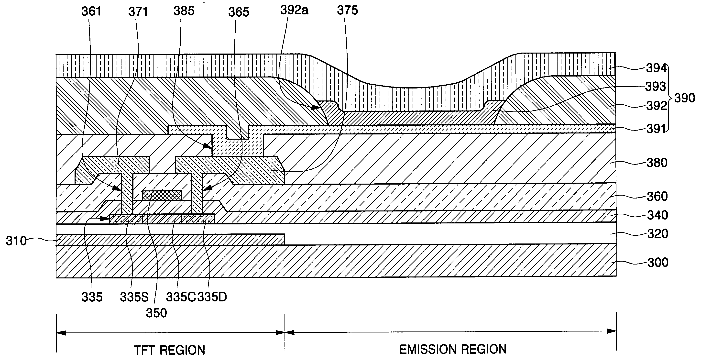
[0046]FIG. 3 shows a cross-sectional view for explaining a flat panel display having a thin film transistor in accordance with a second embodiment of the present invention.

[0047] A flat panel display with a thin film transistor in accordance with the second embodiment may have a structure similar to that having a thin film transistor in accordance with the first embodiment except that a crystallization inducing metal layer 310 may be formed only in the TFT region of the flat panel display. In other words the crystallization inducing metal layer 310 may not, in this example, overlap with the light transmission region of the flat panel display. In such a case, the crystallization inducing metal layer 310 formed only in the TFT region may act to form MIC polycrystalline silicon of an active layer 335 and may also act as a light blocking (or shielding) layer for improving contrast of the flat panel display.

[0048] In addition, an active matrix flat panel display in accordance with the ...


PUM


Abstract

Provided is a thin film transistor that may be manufactured using Metal Induced Crystallization (MIC) and method for fabricating the same. Also provided is an active matrix flat panel display using the thin film transistor, which may be created by forming a crystallization inducing metal layer below a buffer layer and diffusing the crystallization inducing metal layer. The thin film transistor may include a crystallization inducing metal layer formed on an insulating substrate, a buffer layer formed on the crystallization inducing metal layer, and an active layer formed on the buffer layer and including source / drain regions, and including polycrystalline silicon crystallized by the MIC process.

Description

CROSS-REFERENCE TO RELATED APPLICATION [0001] This application claims the benefit of Korea Patent Application No. 2003-85247 filed on Nov. 27, 2003, the disclosure of which is hereby incorporated herein by reference in its entirety. BACKGROUND OF THE INVENTION [0002] (a) Field of the Invention [0003] The present invention relates to a thin film transistor using a Metal Induced Crystallization (MIC) process and method for fabricating the same, and an active matrix flat panel display using the thin film transistor. More particularly, the invention relates to a thin film transistor using a Metal Induced Crystallization (MIC) process and method for fabricating the same. The invention also relates to an active matrix flat panel display using the thin film transistor, which is formed by the method including forming a crystallization inducing metal layer beneath a buffer layer to diffuse the crystallization inducing metal layer. [0004] (b) Description of the Related Art [0005] A method for...

Claims


Application Information

Patent Timeline
02 Jun 2005
Publication
US20050116292A1
IPC
H01L21/00; H01L21/20; H01L21/77; H01L21/84; G02F1/136; H01L27/01; H01L27/12; H01L29/786; H01L31/0392
CPC
H01L21/02422; H01L21/02532; H01L27/1277; H01L27/12; H01L29/78603; H01L21/02672; G02F1/136
Inventors
KOO, JAE-BON; LEE, SANG-GUL