Antenna device suitable for miniaturization

a technology of antenna device and antenna plate, which is applied in the structure of antenna earthing, resonant antenna, radiating element, etc., can solve the problems of increasing material cost or assembling cost, lowering antenna efficiency, increasing manufacturing cost, etc., and achieves the effect of suppressing the effects of dielectric loss, increasing capacitance, and reducing the size of the resonance frequency and the radiating conductor pla

Inactive Publication Date: 2005-06-02
ALPS ALPINE CO LTD
View PDF7 Cites 41 Cited by
  • Summary
  • Abstract
  • Description
  • Claims
  • Application Information

AI Technical Summary

Benefits of technology

[0032] Moreover, the antenna device further comprises chip-type capacitors each composed of a dielectric and electrodes provided on both surfaces of the dielectric, and the chip-type capacitors are arranged between the ground conductor plate and the electrode portions of the first extending portions, respectively. In addition, one electrode of each of the chip-type capacitors is connected to the respective first extending portions, and the other electrodes of the chip-type capacitors are connected to the ground conductor plate. In this way, it is possible to increase capacitance and to reduce a resonance frequency and the size of the radiating conductor plate. In addition, since the dielectric of the chip-type capacitor may be a thin dielectric plate, it is possible to greatly suppress the effects of a dielectric loss.
[0033] Further, the antenna device further comprises chip-type capacitors each composed of a dielectric and electrodes provided on both surfaces of the dielectric, and the chip-type capacitors are arranged between the radiating conductor plate and the electrode portions of the second extending portions, respectively. In addition, one electrode of each of the chip-type capacitors is connected to the radiating conductor plate, and the other electrodes of the chip-type capacitors are connected to the respective electrode portions of the second extending portions. In this way, it is possible to increase capacitance and to reduce a resonance frequency and the size of the radiating conductor plate. In addition, since the dielectric of the chip-type capacitor may be a thin dielectric plate, it is possible to greatly suppress the effects of the dielectric loss.
[0034] Furthermore, the first extending portions each have a leg portion extending from the radiating conductor plate toward the ground conductor plate and an electrode portion provided at an end portion of the leg portion to extend substantially parallel to the ground conductor plate, and the second extending portions each have a leg portion extending from the ground conductor plate toward the radiating conducto

Problems solved by technology

However, in the conventional antenna device, a dielectric loss occurs by the four supporting members 54 where a strong electric field is applied, which results in the lowering of antenna efficiency.
In addition, since the four supporting members 54 made of a dielectric material are arranged between the ground conductor 52 and the radiating conductor plate 53, a material cost or an assembling cost therefor increases, resulting in an increase in manufacturing costs.
Further, since the radiating conductor plate 53 has a rectangular shape, the size thereof increases, which is not suitable for miniaturization.
Therefore, the conventional antenna d

Method used


Image

  • Antenna device suitable for miniaturization
  • Antenna device suitable for miniaturization
  • Antenna device suitable for miniaturization

Examples


first embodiment

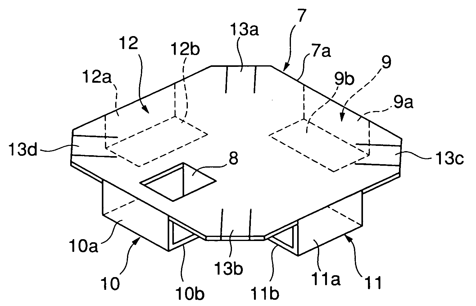
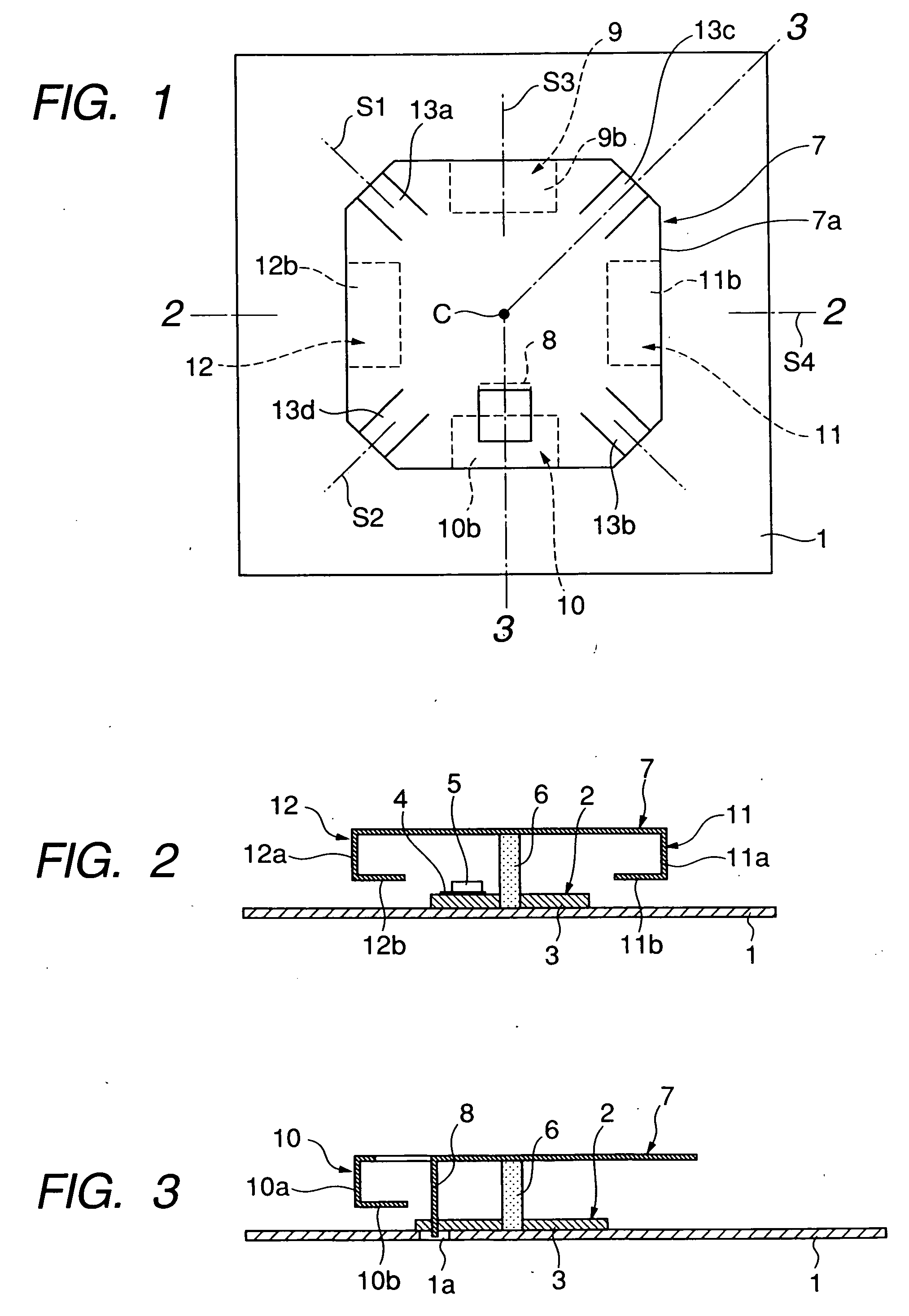
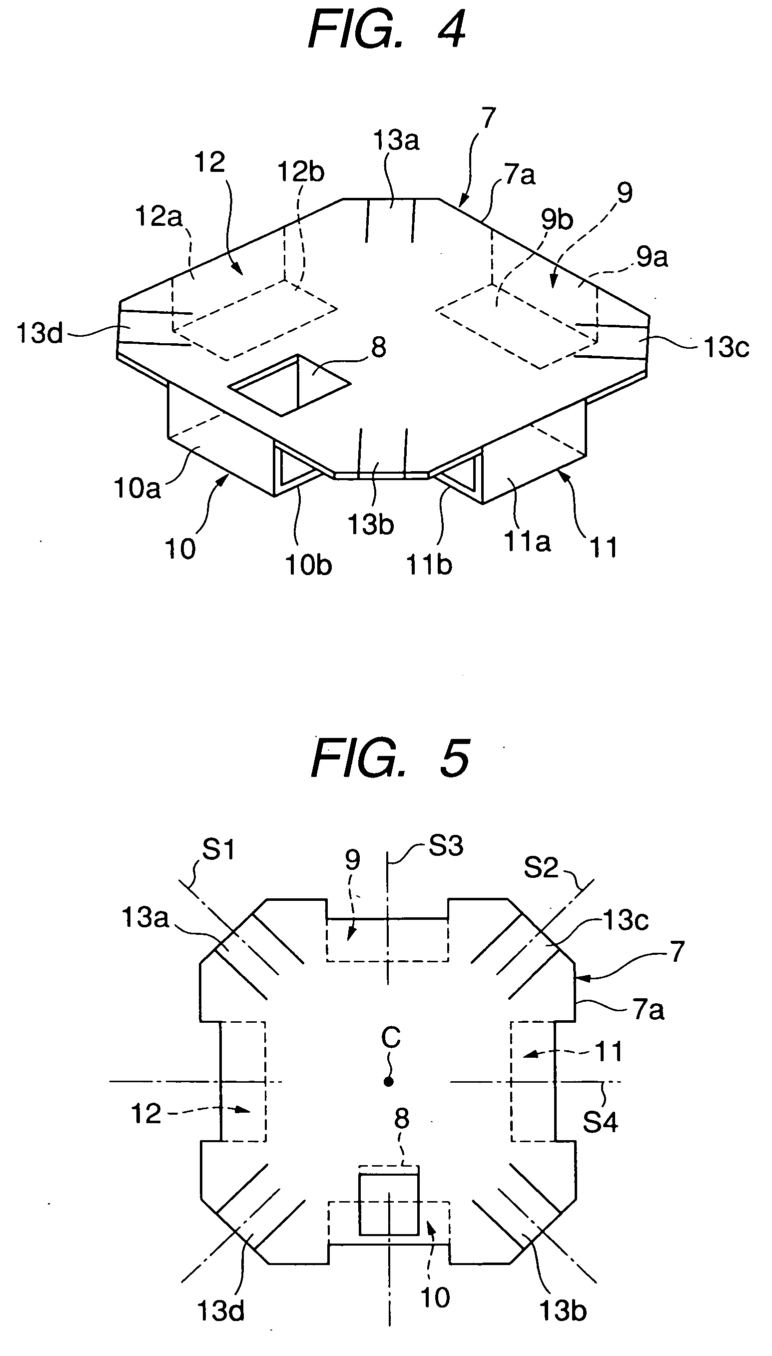
[0054] Hereinafter, the antenna device according to the present invention will be described with reference to FIGS. 1 to 4. A ground conductor plate 1 composed of a metal plate, which is a ground conductor, is formed of a relatively large iron plate having a rectangular shape and has a release hole 1a at an appropriate position.

[0055] A rectangular circuit board 2 includes an insulating plate 3, a wiring pattern 4 provided in the insulating plate 3, and various electronic components 5 mounted on the insulating plate 3. A desired electric circuit comprising a filter circuit, an amplifying circuit, etc., is formed on the circuit board 2.

[0056] The circuit board 2 is mounted on almost the center of the ground conductor plate 1 by appropriate means.

[0057] A supporting member 6 is formed of a pillar portion made of an insulating material or a metallic material. The supporting member 6 passes through the circuit board 2 and is fixed to the center of the ground conductor plate 1.

[0058] ...

third embodiment

[0077] In the third embodiment, capacitance is also formed between the second extending portions 14 to 17 and the radiating conductor plate 7, respectively, and it is possible to adjust the capacitance by bending the leg portions 14a to 17a and / or the electrode portions 14b to 17b of the second extending portions 14 to 17.

[0078] In the present embodiment, structures other than the above-mentioned structure are the same as those in the first embodiment. In addition, the same components as those in the first embodiment have the same reference numerals, and a description thereof will be omitted.

[0079] Further, FIG. 9 illustrates an antenna device according to a fourth embodiment of the present invention. In the fourth embodiment, the first extending portions 9 to 12 are provided in the radiating conductor plate 7, and the second extending portions 14 to 17 are provided in the ground conductor plate 1. In addition, capacitance is formed between the first extending portions 9 to 12 and ...


PUM


Abstract

An antenna device includes a ground conductor plate composed of a metal plate and a radiating conductor plate composed of a metal plate and arranged at a predetermined gap from the ground conductor plate. First extending portions are provided in the radiating conductor plate to extend toward the ground conductor plate, and/or second extending portions are provided in the ground conductor plate to extend toward the radiating conductor plate. Capacitance is formed between the first extending portions and the ground conductor plate, between the second extending portions and the radiating conductor plate, or the first extending portions and the second extending portions respectively.

Description

BACKGROUND OF THE INVENTION [0001] 1. Field of the Invention [0002] The present invention relates to a patch antenna device suitable for a GPS antenna and the like. [0003] 2. Description of the Related Art [0004] A conventional antenna device will be described with reference to the accompanying figures. FIG. 13 is a plan view of the conventional antenna device, and FIG. 14 is a cross-sectional view illustrating the main parts of the conventional antenna device. [0005] Next, the structure of the conventional antenna device will be described with reference to FIGS. 13 and 14. The conventional antenna device comprises a ground conductor 52 patterned on an insulating substrate 51, a radiating conductor plate 53 composed of a metal plate and arranged parallel to the ground conductor 52 at a predetermined gap therefrom, and four supporting members 54 made of a dielectric material and provided on the ground conductor 52. [0006] Further, the radiating conductor plate 53 has a square shape, ...

Claims


Application Information

Patent Timeline
IPC IPC(8): H01Q1/24H01Q13/08H01Q9/04H01Q23/00
CPCH01Q1/243H01Q23/00H01Q9/0442H01Q9/0414
Inventor YUANZHU, DOUSUZUKI, TOMOTAKA
Owner ALPS ALPINE CO LTD
Why Eureka
Try Eureka