Light sensing element, array substrate having the same and liquid crystal display apparatus having the same

a technology of light sensing elements and array substrates, which is applied in the direction of instruments, radiation controlled devices, optical radiation measurement, etc., can solve the problems of signal interference between the elements in the pixel region, the light sensing element may not have enough space, and the yield of the lcd apparatus may decrease, so as to achieve the effect of simplifying the structure of the lcd panel and increasing the opening ratio

Active Publication Date: 2005-06-02
SAMSUNG DISPLAY CO LTD
View PDF1 Cites 59 Cited by
  • Summary
  • Abstract
  • Description
  • Claims
  • Application Information

AI Technical Summary

Benefits of technology

[0022] Therefore, the LCD panel includes one light sensing thin film transistor (TFT) corresponding to one pixel so that structure of the LCD panel is simplified and opening ratio is increased.

Problems solved by technology

A pixel region of the array substrate is not small so that the light sensing element may not have enough space on the array substrate.
In addition, a number of elements formed in one pixel region of the array substrate is increased so that the structure of the array substrate is complicated, thereby decreasing a yield of the LCD apparatus.
Furthermore, a signal interference may be generated between the elements in the pixel region.

Method used


Image

  • Light sensing element, array substrate having the same and liquid crystal display apparatus having the same
  • Light sensing element, array substrate having the same and liquid crystal display apparatus having the same
  • Light sensing element, array substrate having the same and liquid crystal display apparatus having the same

Examples


Embodiment Construction

[0036] Hereinafter, the present invention will be described in detail with reference to the accompanying drawings.

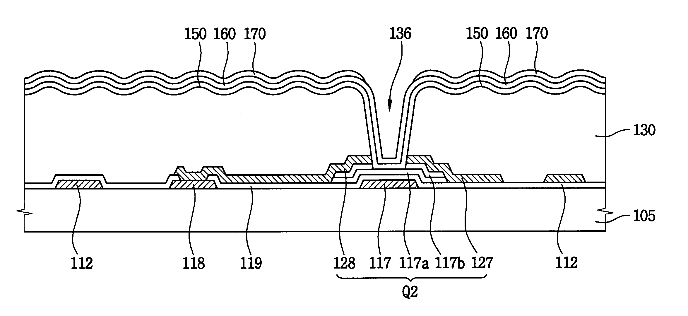
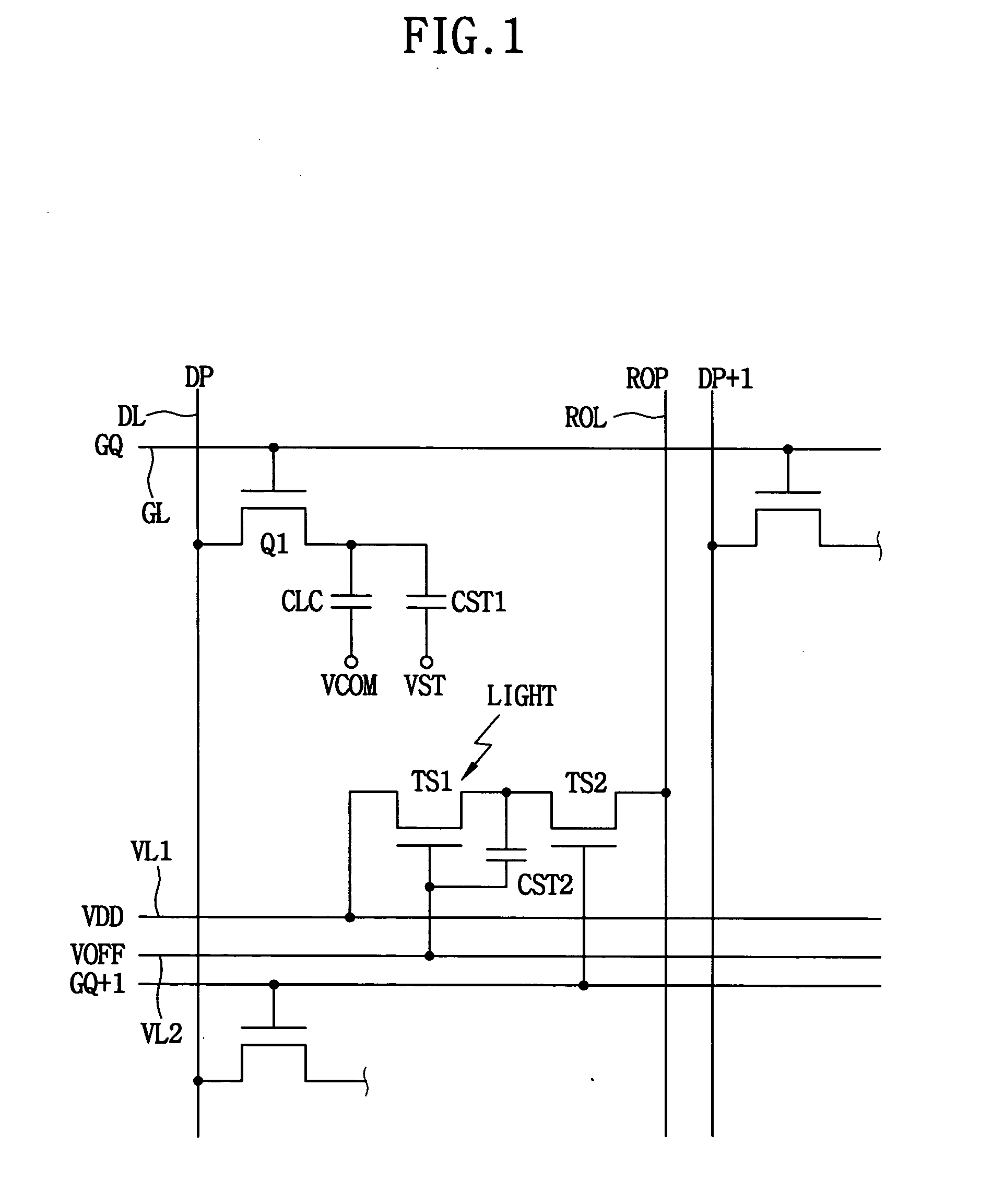
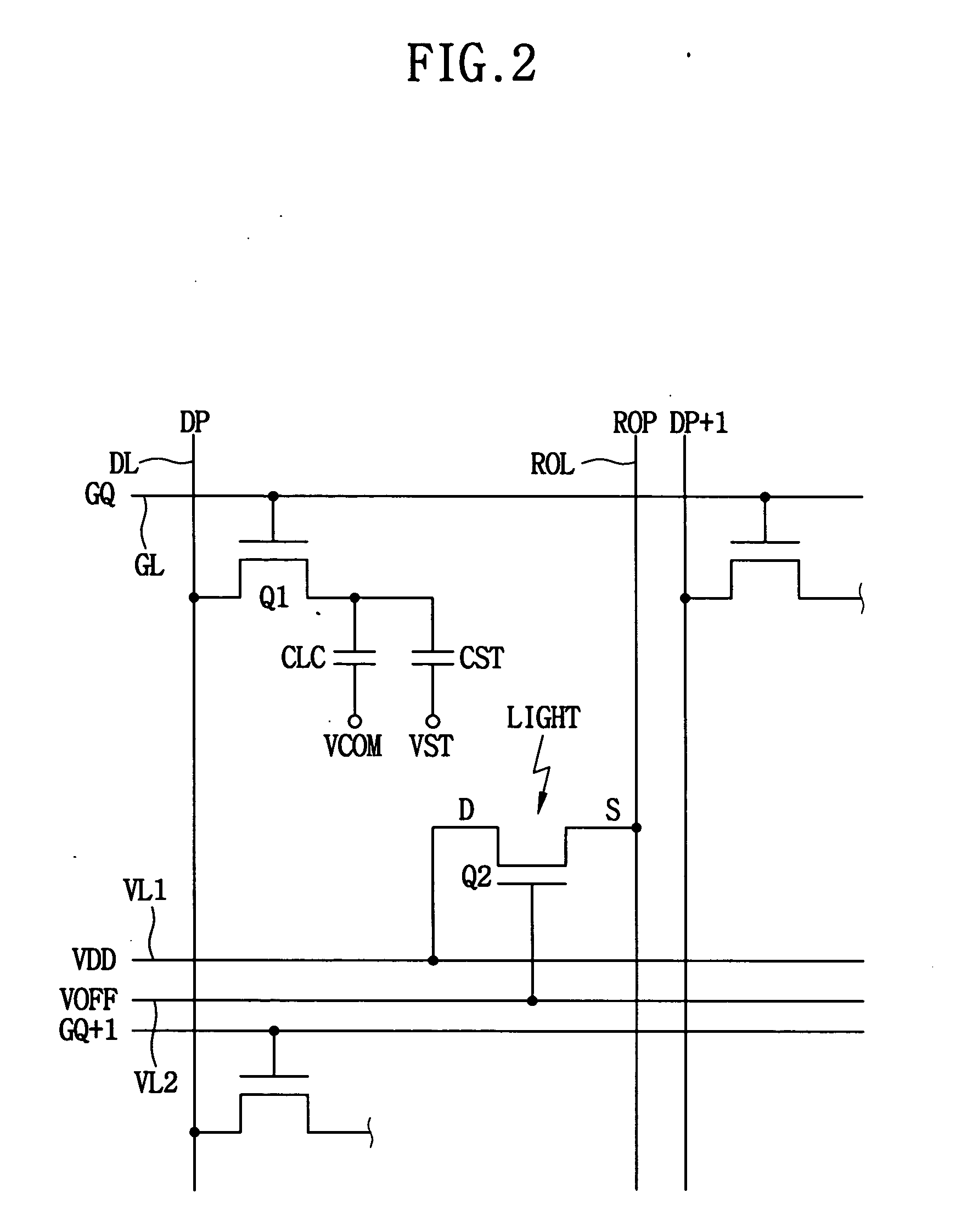
[0037]FIG. 1 is a circuit diagram showing a light sensing element of an LCD panel in accordance with an exemplary embodiment of the present invention. The light sensing element is disposed in a pixel region of the LCD panel.

[0038] Referring to FIG. 1, the LCD panel includes a gate line GL, a data line DL, a first switching element Q1 electrically connected to the gate and data lines GL and DL, a liquid crystal capacitor CLC electrically connected to the first switching element Q1 and a first storage capacitor CST1. The LCD panel may include a plurality of the gate lines GL, a plurality of the data lines DL, a plurality of the first switching elements Q1, a plurality of the liquid crystal capacitors CLC and a plurality of the first storage capacitors CST1. The LCD panel further includes a first power supply line VL1, a second power supply line VL2, a second switching el...


PUM

PropertyMeasurementUnit
bias voltageaaaaaaaaaa

Abstract

In a light sensing element having simplified structure, an array substrate having the light sensing element and an LCD apparatus having the light sensing element, the light sensing element includes a first electrode, a control electrode and a second electrode. An alternating bias voltage is applied to the first electrode. An off voltage is applied to the control electrode. The second electrode outputs a light-induced leakage current based on an externally provided light and the bias voltage. Therefore, the array substrate includes one light sensing switching element corresponding to one pixel so that structure of the array substrate is simplified and opening ratio is increased.

Description

CROSS-REFERENCE OF RELATED APPLICATIONS [0001] The present application claims priority from Korean Patent Application No. 2003-74317, filed on Oct. 23, 2003, the disclosure of which is hereby incorporated herein by reference in its entirety. BACKGROUND OF THE INVENTION [0002] 1. Field of the Invention [0003] The present invention relates to a light sensing element, an array substrate having the light sensing element and a liquid crystal display (LCD) apparatus having the light sensing element. More particularly, the present invention relates to a light sensing element having a simple structure and an improved opening ratio, an array substrate having the light sensing element and an LCD apparatus having the light sensing element. [0004] 2. Description of the Related Art [0005] Generally, a light sensing element senses a light that is provided from an exterior to an electronic apparatus so as to sense a position where the light is incident. A liquid crystal display (LCD) apparatus hav...

Claims


Application Information

Patent Timeline
Patent Type & Authority Applications(United States)
IPC IPC(8): G01J1/02G01J1/44G02F1/133G02F1/1333G02F1/1335G02F1/1343G02F1/1362G02F1/1368G06F3/041G06F3/042H01L21/336H01L27/146H01L29/786H01L31/10
CPCG02F1/13338G02F1/133555H01L27/14603G02F2001/13312G02F1/1362G02F1/13312G02F1/1368
Inventor PAK, SANG-JINKIM, HYUNG-GUELUH, KEE-HANCHO, JONG-WHANJEON, JINJUNG, YOUNG-BAE
Owner SAMSUNG DISPLAY CO LTD
Why Eureka
Try Eureka