In-plane switching mode active matrix type liquid crystal display device and method of fabricating the same
a liquid crystal display and active matrix technology, applied in the direction of identification means, instruments, optics, etc., can solve the problem of preventing the electrode from being properly driven, and achieve the effect of increasing the aperture ratio
- Summary
- Abstract
- Description
- Claims
- Application Information
AI Technical Summary
Benefits of technology
Problems solved by technology
Method used
Image
Examples
first embodiment
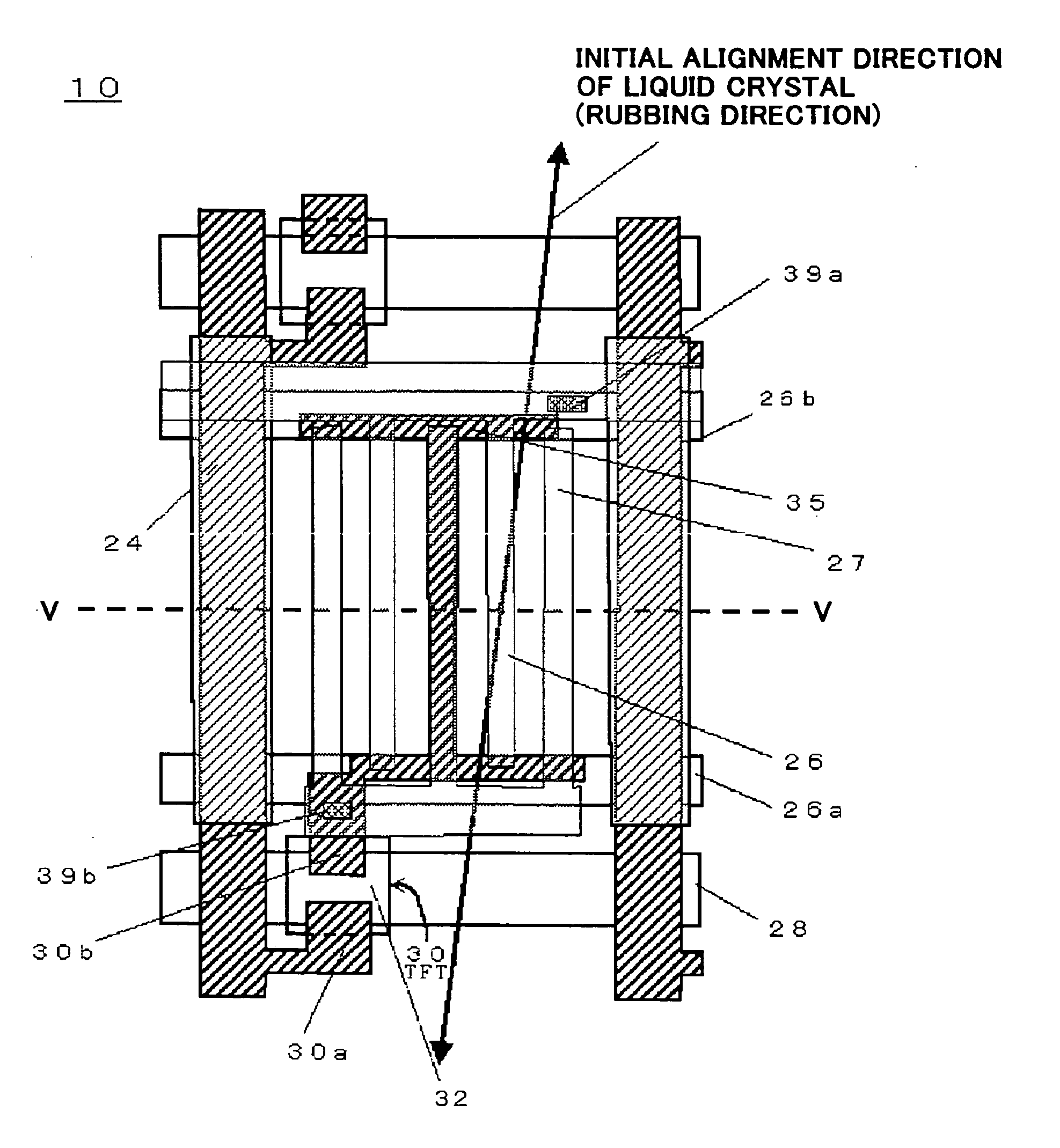
[0278]FIGS. 4, 5 and 6 illustrate an in-plane switching mode active matrix type liquid crystal display device in accordance with the first embodiment of the present invention. FIG. 4 is a plan view of the liquid crystal display device 10 in accordance with the first embodiment, FIG. 5 is a cross-sectional view taken along the line V-V in FIG. 4, and FIG. 6 is a circuit diagram of a unit pixel.
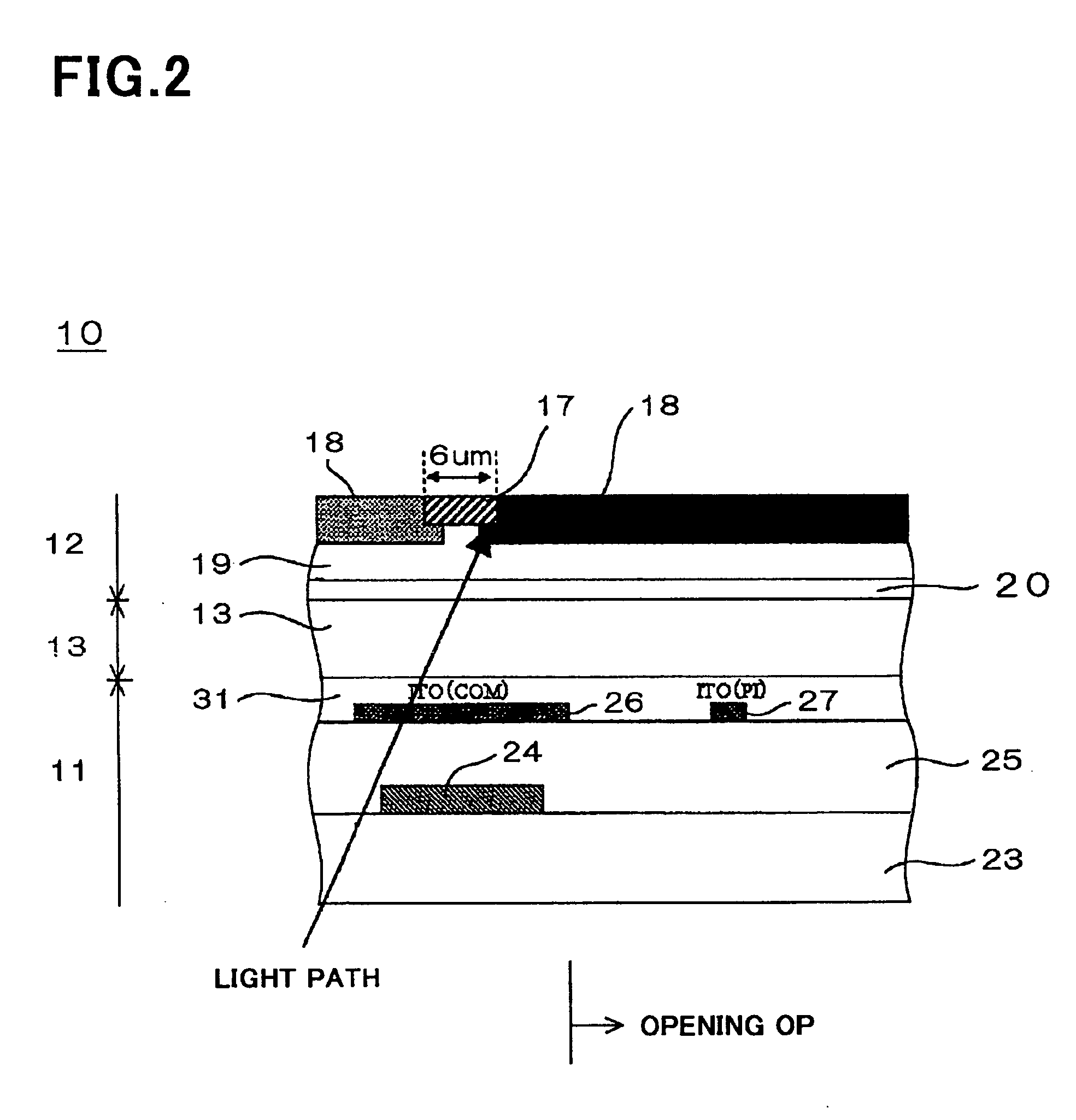
[0279] As illustrated in FIG. 5, the liquid crystal display device 10 is comprised of an active device substrate 11, an opposing substrate 12, and a liquid crystal layer 13 sandwiched between the active device substrate 11 and the opposing substrate 12.
[0280] The opposing substrate 12 includes an electrically insulating transparent substrate 16, a black matrix layer 17 formed on a first surface of the electrically insulating transparent substrate 16 as a light-impermeable film, a color layer 18 formed on the first surface of the electrically insulating transparent substrate 16 such that the c...
first example
[0434]FIGS. 33A to 33J are cross-sectional views of the liquid crystal display device 10, illustrating respective steps of the first example of the method of fabricating the liquid crystal display device 10 including the second interlayer insulating film 25 having a multi-layered structure of an inorganic film and an organic film.
[0435] First, as illustrated in FIG. 33A, a chromium layer as the first metal layer is formed on a glass substrate as the electrically insulating transparent substrate 22, and then, is patterned by photolithography and dry etching into the common electrode lines 26a and 26b and the scanning line 28 in both the common electrode line terminal 41e and the scanning line terminal 41c.
[0436] Though only the common electrode line 26b is illustrated in FIGS. 33A to 35H, the common electrode line 26a together with the common electrode line 26b will be explained hereinbelow, because the common electrode line 26a is formed together with the common electrode line 26b...
second example
[0447]FIGS. 34A to 34I are cross-sectional views of the liquid crystal display device 10, illustrating respective steps of the second example of the method of fabricating the liquid crystal display device 10 including the second interlayer insulating film 25 comprised singly of an organic film.
[0448] First, as illustrated in FIG. 34A, a chromium layer as the first metal layer is formed on a glass substrate as the electrically insulating transparent substrate 22, and then, is patterned by photolithography and dry etching into the common electrode lines 26a and 26b and the scanning line 28 in both the common electrode line terminal 41e and the scanning line terminal 41c.
[0449] Then, as illustrated in FIG. 34B, the first interlayer insulating film 23 is formed all over the transparent substrate 22, covering the common electrode lines 26a and 26b and the scanning line 28 therewith. The first interlayer insulating film 23 has a multi-layered structure of a silicon dioxide (SiO2) film a...
PUM
 Abstract
Description
Claims
Application Information


