

Semiconductor storage device
- Summary
- Abstract
- Description
- Claims
- Application Information
AI Technical Summary
Benefits of technology
Problems solved by technology
Method used
Image

Examples
Embodiment Construction
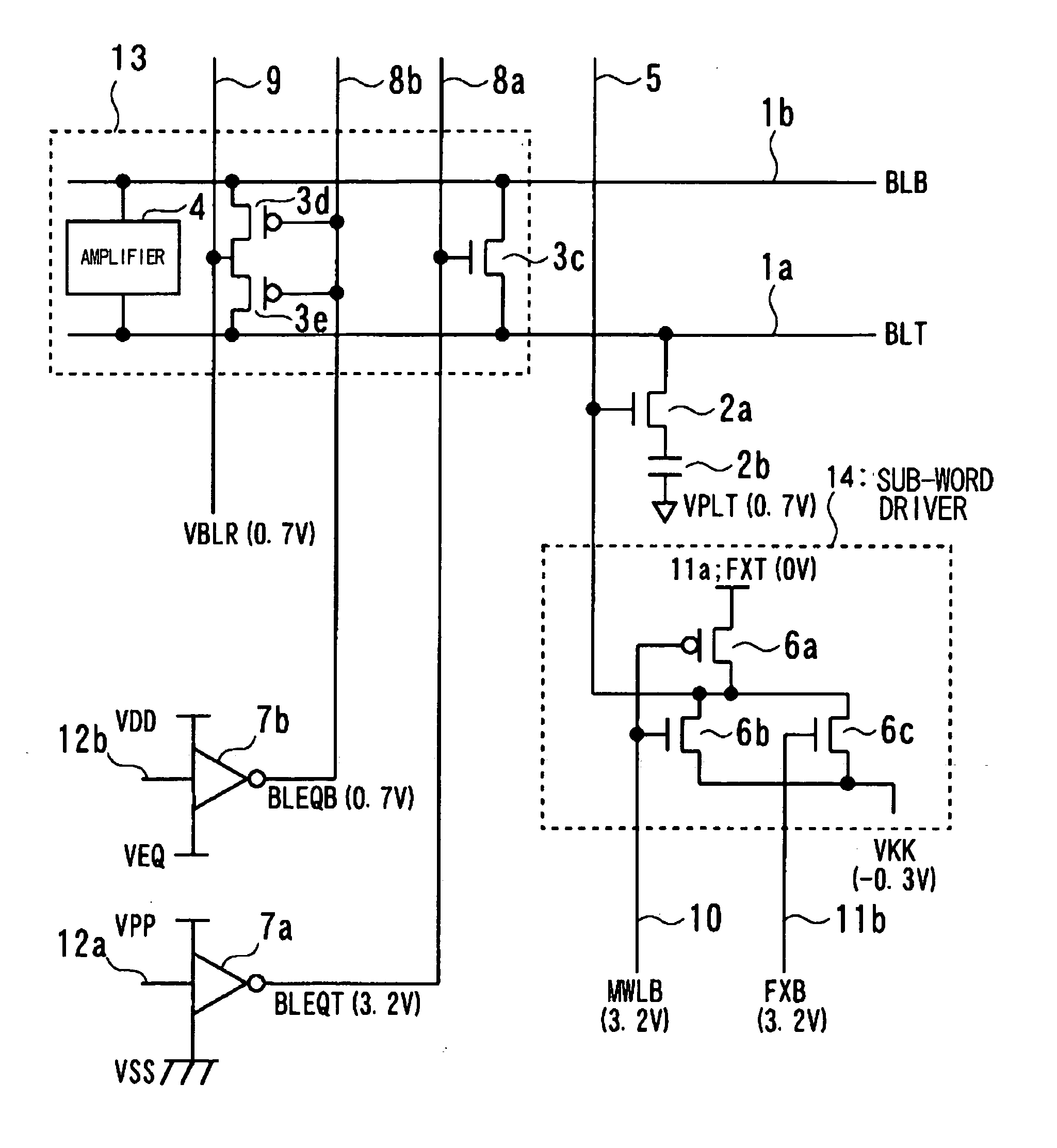
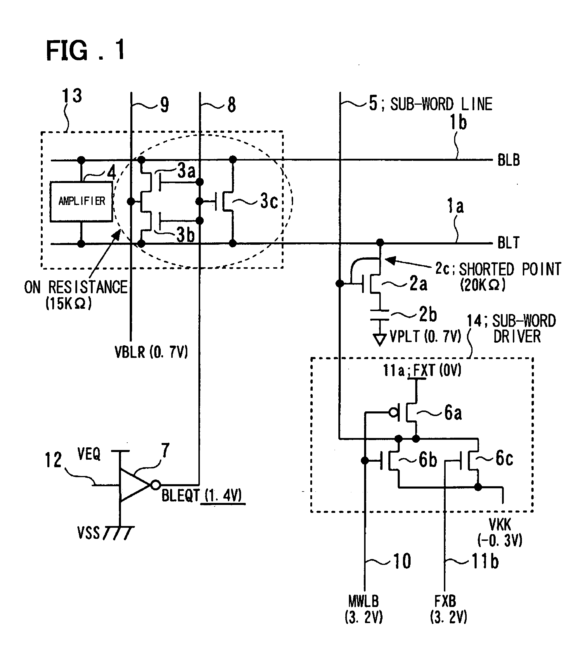
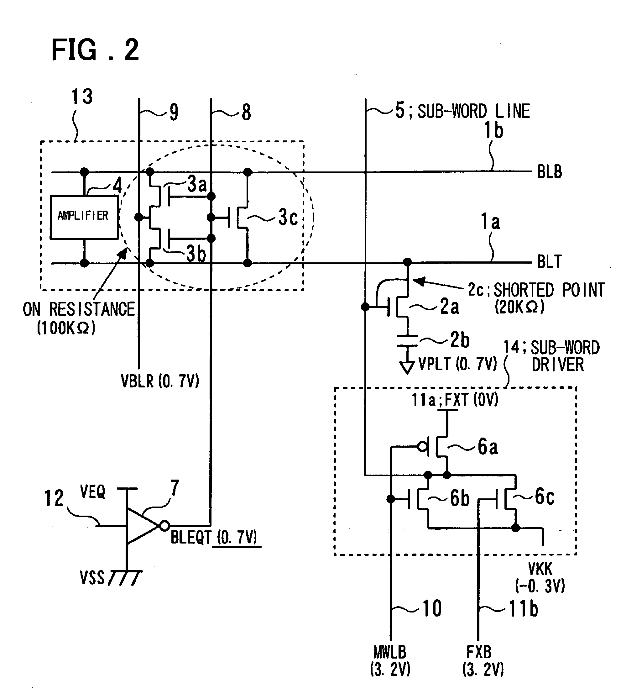
[0041] For further detailed description of the present invention, reference is made to the accompanying drawings. The semiconductor storage device, according to a preferred embodiment of the present invention, is configured to control the potential at the control terminal of a transistor, forming a precharge equalizing circuit, supplying the precharge potential to the bit line, during the low power (power-down) operation, is controlled to supply a preset potential, varied from the potential applied to the control terminal during the precharging of the normal operation (e.g. a high potential VPP). According to the present invention, the on-current on the transistor control terminal is reduced by reducing the current supplied to the bit line to reduce the leakage current across the bit and word lines. During the normal operation, other than the low power operation, the potential sufficient to turn on the transistor is supplied to the control terminal of the transistor forming the prec...
PUM
 Abstract
Description
Claims
Application Information