Process for forming an electrically conductive interconnect

a technology of electrically conductive interconnects and metallic interconnects, which is applied in the direction of basic electric elements, electrical apparatus, semiconductor/solid-state device manufacturing, etc., to achieve the effect of reducing field-induced metal contamination of dielectrics

Inactive Publication Date: 2005-06-02
IBM CORP
View PDF15 Cites 47 Cited by
  • Summary
  • Abstract
  • Description
  • Claims
  • Application Information

AI Technical Summary

Benefits of technology

[0007] The present invention relates to a process that makes it possible to reduce field induced metal contamination of dielectric by metallic interconnect in a via and / or leakage failure of the metallic interconnect. The present invention relates to a process for forming an electrically conductive metallic interconnect in a via in a dielectric.

Problems solved by technology

When the Ta is subsequently deposited and sputter etched the bottom of the trenches are poorly covered such that the Cu that is later deposited is able to escape through the defected liner into the dielectric causing failure.

Method used


Image

  • Process for forming an electrically conductive interconnect
  • Process for forming an electrically conductive interconnect
  • Process for forming an electrically conductive interconnect

Examples


Embodiment Construction

[0027] In order to facilitate an understanding of the present invention, reference is made to the figures.

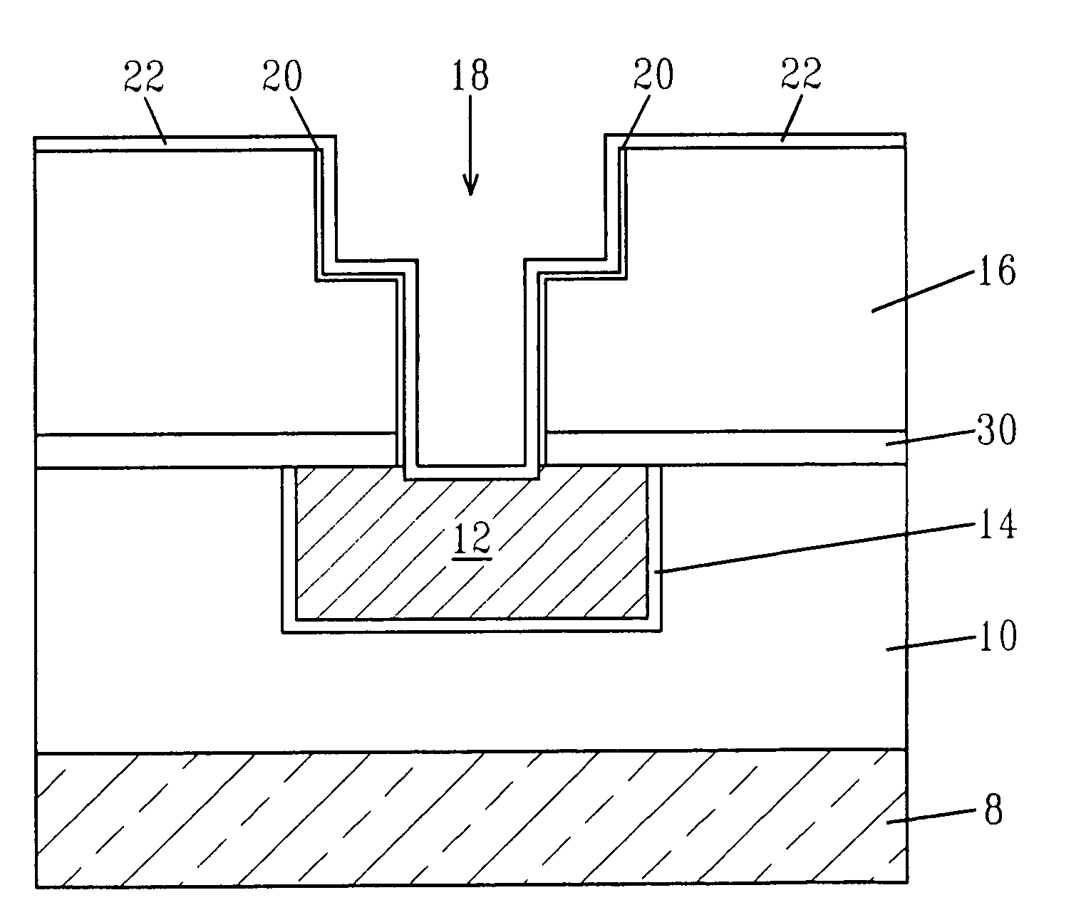
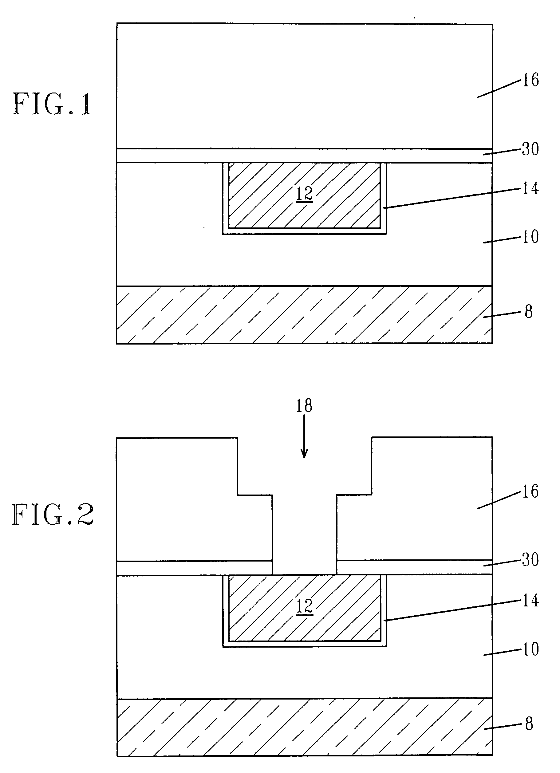
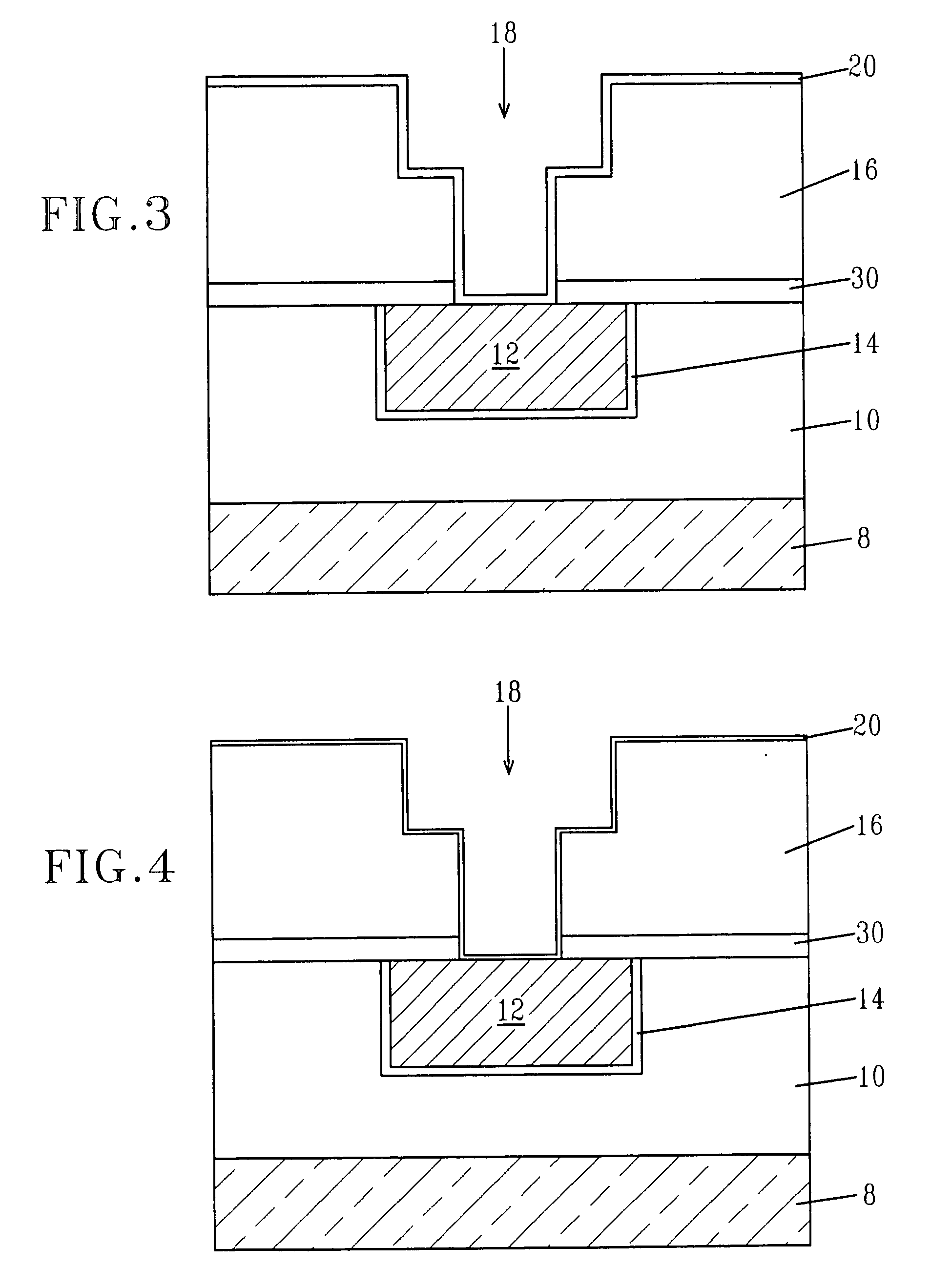
[0028] According to the present invention dielectric layers 10 and 16 are provided on a semiconductive substrate 8 such as silicon, silicon-germanium alloys, and silicon carbide or gallium arsenide. The dielectric layer 10 contains electrically conductive lines 12 and can contain a barrier or liner 14 on the bottom and sidewalls the conductive lines 12. Also, typically a capping layer 30 such as silicon nitride is provided on the conductive lines 12. See FIG. 1. Examples of dielectric layers 10 and 16 are silicon dioxide (SiO2), phosphosilicate glass (PSG), boron doped PSG (BDPSG) or tetraethylorthosilicate (TEOS), and more typically low-k dielectrics having a dielectric constant of less than 3.9 such as SILK(available from Dow Chemical), SiCH(available from AMAT under the trade designation BLOK), SiCOH(available from Novellus under the trade designation Coral, from AMAT under ...


PUM


Abstract

An electrically conductive metallic interconnect in a trench or via in a dielectric is provided by depositing a first liner layer on the walls and bottom of the trench or via; removing residual contamination from the bottom of the trench or via; depositing a second liner layer in the trench; depositing a seed layer and filling the trench with electrically conductive metallic material.

Description

TECHNICAL FIELD [0001] The present invention relates to a process for forming an electrically conductive metallic interconnect in a via in a dielectric. More particularly, the present relates to reducing field induced metal contamination of the dielectric and / or leakage failure of the metallic interconnect. The present invention is of especial significance when the dielectric is a low-k dielectric. BACKGROUND OF INVENTION [0002] Copper is presently the preferred material choice for forming interconnects in integrated circuits. Copper replaced aluminum and AlCu alloys due to lower resistance and better resilience to electromigration. The advantage of copper metallization has been recognized by the entire semiconductor industry. Copper metallization has been the subject of extensive research documented by two entire issues of the Materials Research Society (MRS) Bulletin. One dedicated to academic research on the subject is MRS Bulletin, Vol. XVIII, No. 6 (June 1993) and the other ded...

Claims


Application Information

Patent Timeline
Patent Type & Authority Applications(United States)
IPC IPC(8): H01L21/768
CPCH01L21/76805H01L21/76846H01L21/76844
Inventor CHIRAS, STEFANIE R.LANE, MICHAEL W.ROSENBERG, ROBERTSPOONER, TERRY A.
Owner IBM CORP
Why Eureka
Try Eureka