
Wafer processing machine

a processing machine and wafer technology, applied in the direction of lapping machines, grinding machine components, manufacturing tools, etc., can solve problems such as the breakage of the wafer

Active Publication Date: 2005-06-02
DISCO CORP
View PDF8 Cites 38 Cited by
  • Summary
  • Abstract
  • Description
  • Claims
  • Application Information

AI Technical Summary

Benefits of technology

[0012] Preferably, the wafer processing machine has an air brush means for removing grinding chips adhered to the ground surface of a wafer held on a chuck table when the chuck table is moved from the grinding areas to the polishing area by the turning of the turntable. Preferably, the air brush means is mounted on the grinding chamber cover means for forming the grinding chamber. Preferably, the air brus...

Problems solved by technology

However, there is a problem that when the wafer ground by a grinding machine is carried to an etching machine or polishing machine from the grinding machine to subject it to etching or polishing, the wafer may be broken.

Method used


Image

  • Wafer processing machine
  • Wafer processing machine
  • Wafer processing machine

Examples


Embodiment Construction

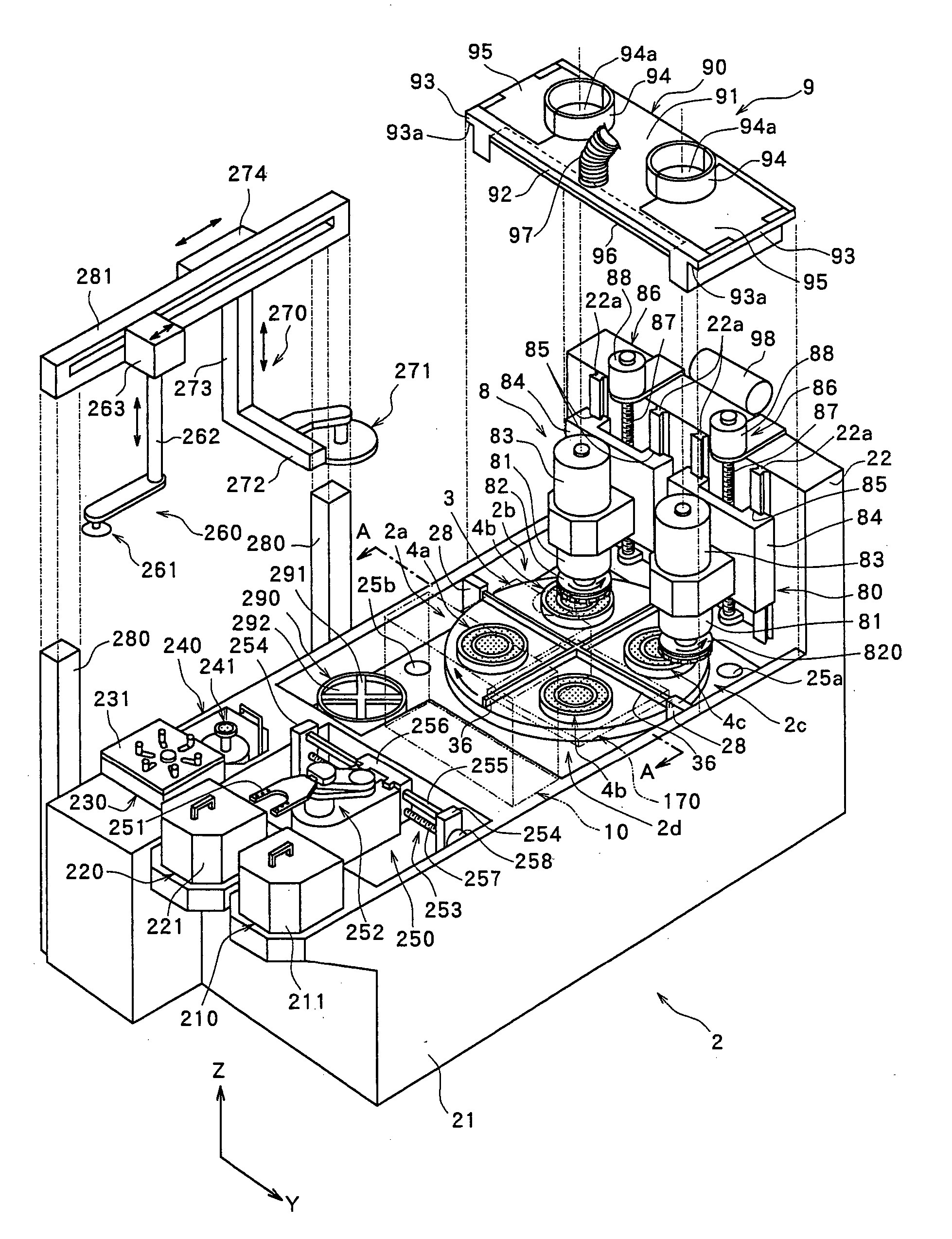
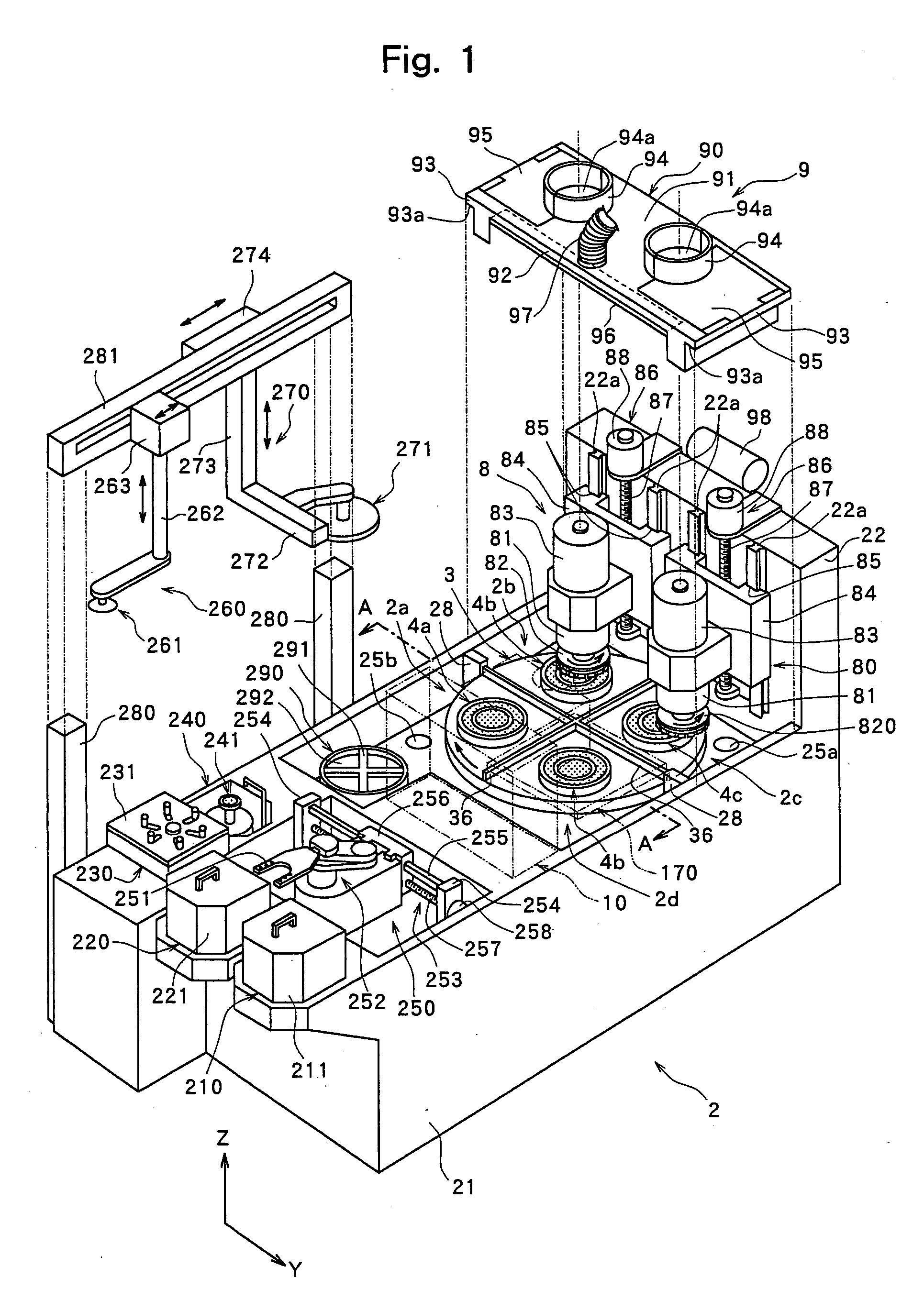
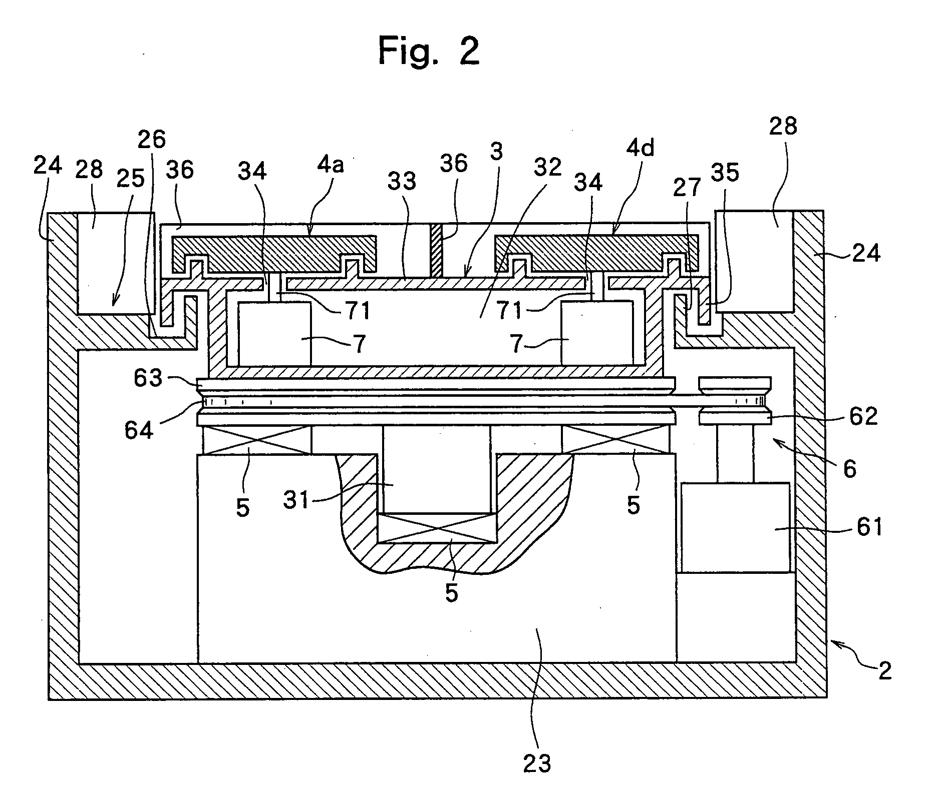
[0030] A wafer processing machine according to a preferred embodiment of the present invention will be described in detail hereinunder with reference to the accompanying drawings.

[0031]FIG. 1 is a perspective view of a wafer processing machine constituted according to the present invention.

[0032] The wafer processing machine shown in FIG. 1 comprises a housing denoted as a whole by numeral 2. The housing 2 contains a rectangular parallelepiped main portion 21 extending long and narrow and an upright wall 22 that is disposed at the back end portion (upper right portion in FIG. 1) of the main potion 21 and extends upward in a substantially vertical direction therefrom. This housing 2 has a workpiece take-in / take-out area 2a where a wafer as a workpiece later described is taken in and out, a rough grinding area 2b, a finish grinding area 2c and a polishing area 2d.

[0033] A turntable 3 is turnably mounted on the main portion 21 of the above housing 2 and turned along the above take-i...


PUM

PropertyMeasurementUnit
Angleaaaaaaaaaa
Flexibilityaaaaaaaaaa
Areaaaaaaaaaaa

Abstract

A wafer processing machine comprising a turntable, a plurality of chuck tables mounted on the turntable, a grinding means for grinding a wafer held on the chuck table, and a multipurpose polishing means for polishing the ground surface of a wafer held on a chuck table, wherein the multipurpose polishing means comprises a mounter for detachably mounting a polishing tool, a spindle unit for rotating the mounter, a spindle unit support means for supporting the spindle unit in such a manner that the spindle unit can move in a direction perpendicular to the holding surfaces of the chuck tables and in a direction parallel to the holding surfaces of the chuck tables, a first polishing-feed means for moving the spindle unit in a direction perpendicular to the holding surfaces of the chuck tables, and a second polishing-feed means for moving the spindle unit in a direction parallel to the holding surfaces of the chuck tables.

Description

FIELD OF THE INVENTION [0001] The present invention relates to a wafer processing machine for processing the surface of a wafer such as a semiconductor wafer or an optical device wafer. DESCRIPTION OF THE PRIOR ART [0002] In the production process of a semiconductor device, a large number of rectangular areas are sectioned by cutting lines called “streets” arranged in a lattice pattern on the front surface of a substantially disk-like semiconductor wafer, and a semiconductor circuit is formed in each of the rectangular areas. Individual semiconductor chips are manufactured by dividing this semiconductor wafer having a large number of semiconductor circuits along the streets. An optical device wafer comprising optical devices composed of gallium nitride-based compound semiconductors laminated in a plurality of areas that are sectioned by streets formed in a lattice pattern on the front surface of a sapphire substrate is also divided into optical devices such as light emitting diodes ...

Claims


Application Information

Patent Timeline
IPC IPC(8): B24B7/22B24B7/24B24B37/04H01L21/304
CPCB24B37/345B24B7/228
Inventor MIZOMOTO, YASUTAKAYAMAHATA, ICHIROGOTO, TOSHIMITSUIZUMITA, MASANORIIIZUKA, KATSUNORIYASUDA, SHINJI
Owner DISCO CORP
Learn More