Apparatus and method for inspecting and repairing a circuit defect

a liquid crystal display device and apparatus technology, applied in the direction of printed circuit repair/correction, manufacturing tools, welding/soldering/cutting articles, etc., can solve the problems of increasing the risk of defective products rework, occupying the space of cleaning room, and frequent formation of circuit defects, etc., to achieve the effect of reducing the space occupied by inspection and repair machines

Inactive Publication Date: 2005-06-09
AU OPTRONICS CORP
View PDF7 Cites 17 Cited by
  • Summary
  • Abstract
  • Description
  • Claims
  • Application Information

AI Technical Summary

Benefits of technology

[0009] The object of the present invention is to provide an apparatus for inspecting and repairing a circuit defect so that the space occupied by the inspection and repair machines is reduced, and the inspection and repair of circuit defects can be carried out precisely and quickly.

Problems solved by technology

However, some circuit defects like the short defect 30 or the open defect 20 are very frequently formed due to imperfections of process.
In such a conventional procedure, the open / short inspection machine and the laser repair machine are two distinctly separate machines, so the glass substrates have to be transported between the machines which are time-consuming.
Besides, the process line is too long, and merely leads to increases in rework risk of defective products and occupied space of cleaning room.
In addition to that, the glass substrate has to be aligned again in both machines, which not only increases the operation time, but also lowers the whole precision of alignment due to different coordinate systems.
Thus, the use of two separate machines does not benefit the trend of an increasingly narrow line width and the automation of defect inspection and repair.
However, as the substrates have become bigger and bigger, that kind of design will occupy more and more space in both machines.
As a result, the cost in facility will increase, and the precision of the whole procedure will fall.

Method used


Image

  • Apparatus and method for inspecting and repairing a circuit defect
  • Apparatus and method for inspecting and repairing a circuit defect
  • Apparatus and method for inspecting and repairing a circuit defect

Examples


Embodiment Construction

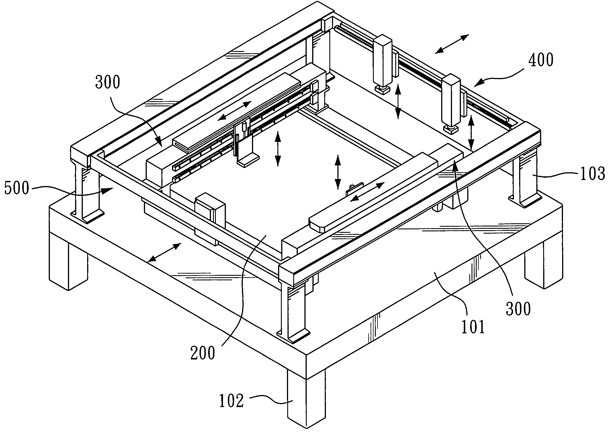
[0028] With reference to FIG. 4, there is shown a perspective view of the apparatus for inspecting and repairing a circuit defect of the present invention. The apparatus has a base 101, a substrate-supporting platform 200, a contact inspection module 300, a non-contact inspection module 400, and a laser repair module 500. Moreover, the base 101 and stands 102 serve as a foundation of the whole apparatus for supporting all the components of the apparatus. The motor supporter 103 is further utilized to support and raise the motors. The substrate-supporting platform 200 substantially resembles a rectangular plate and serves to support and fix a glass substrate. The substrate-supporting platform 200 is usually made of transparent materials, such as glass or acrylate. Moreover, the transparent substrate-supporting platform 200 can improve the contrast of images by mounting a lighting module (not shown in the figure) below the transparent substrate-supporting platform 200 if higher contra...


PUM

PropertyMeasurementUnit
distanceaaaaaaaaaa
movementaaaaaaaaaa
widthaaaaaaaaaa

Abstract

An apparatus for inspecting and repairing a circuit defect is disclosed, which has a base; a substrate-supporting platform mounted on the base; a contact inspection module having at least one contact probe and a first driving-system that drives at least one contact probe to contact the circuits formed on the glass substrate and thereby inspect a circuit defect; a non-contact inspection module having at least one non-contact sensor and a second driving-system that drives at least one non-contact sensor to inspect the circuit defect in a non-contact manner; and a laser repair module having a laser head and a third driving-system that drives the laser head to go to the circuit defect and repair the circuit defect. A method for inspecting and repairing a circuit defect is also disclosed therewith.

Description

BACKGROUND OF THE INVENTION [0001] 1. Field of the Invention [0002] The present invention relates to an apparatus and method for inspecting and repairing circuit defects of a liquid crystal display device and, more particularly, to an apparatus that concurrently has functions of inspecting and repairing circuit defects of a liquid crystal display device. [0003] 2. Description of Related Art [0004] With reference to FIGS. 1 and 2, a plurality of metal lines having a matrix pattern is formed on a glass substrate 10 after the array process of the manufacturing procedure of a liquid crystal display device. The metal lines include the data lines (source lines) 11 and the scan lines 12. However, some circuit defects like the short defect 30 or the open defect 20 are very frequently formed due to imperfections of process. Generally, an open / short inspection machine is used to inspect for those kinds of defects. The inspection method of the open / short inspection machine commonly includes a ...

Claims


Application Information

Patent Timeline
Patent Type & Authority Applications(United States)
IPC IPC(8): B23K26/00B23K26/10H05K3/22
CPCB23K26/0003H05K3/225B23K2201/36B23K26/10B23K26/351B23K2101/36
Inventor LIAO, KUO-TINGLEE, KUO-KUEICHU, CHUN CHIEN
Owner AU OPTRONICS CORP
Why Eureka
Try Eureka